- 您现在的位置:买卖IC网 > PDF目录170346 > CY39050V208-222NTC (CYPRESS SEMICONDUCTOR CORP) LOADABLE PLD, 7 ns, PQFP208 PDF资料下载
参数资料
| 型号: | CY39050V208-222NTC |
| 厂商: | CYPRESS SEMICONDUCTOR CORP |
| 元件分类: | PLD |
| 英文描述: | LOADABLE PLD, 7 ns, PQFP208 |
| 封装: | THERMALLY ENHANCED, QFP-208 |
| 文件页数: | 2/57页 |
| 文件大小: | 1166K |
| 代理商: | CY39050V208-222NTC |
第1页当前第2页第3页第4页第5页第6页第7页第8页第9页第10页第11页第12页第13页第14页第15页第16页第17页第18页第19页第20页第21页第22页第23页第24页第25页第26页第27页第28页第29页第30页第31页第32页第33页第34页第35页第36页第37页第38页第39页第40页第41页第42页第43页第44页第45页第46页第47页第48页第49页第50页第51页第52页第53页第54页第55页第56页第57页
PRELIMINARY
Delta39K ISR
CPLD Family
Document #: 38-03039 Rev. **
Page 10 of 57
.
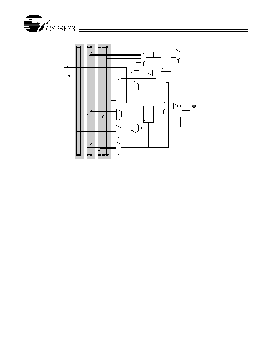
I/O Cell
Figure 8 is a block diagram of the Delta39K I/O cell. The I/O
cell contains a three-state input buffer, an output buffer, and a
register that can be configured as an input or output register.
The output buffer has a slew rate control option that can be
used to configure the output for a slower slew rate. The input
of the device and the pin output can each be configured as
registered or combinatorial; however, only one path can be
configured as registered in a given design.
The output enable can be selected from one of the four global
control signals or from one of two Output Control Channel
(OCC) signals. The output enable can be configured as always
enabled or always disabled or it can be controlled by one of
the remaining inputs to the mux. The selection is done via a
mux that includes VCC and GND as inputs.
One of the global clocks can be selected as the clock for the
I/O cell register. The clock mux output is an input to a clock
polarity mux that allows the input/output register to be clocked
on either edge of the clock.
Slew Rate Control
The ouput buffer has a slew rate control option. This allows the
output buffer to slew at a fast rate (3 V/ns) or a slow rate (1
V/ns). All I/Os default to fast slew rate. For designs concerned
with meeting FCC emissions standards the slow edge pro-
vides for lower system noise. For designs requiring very high
performance the fast edge rate provides maximum system
performance.
Programmable Bus Hold
On each I/O pin, user-programmable-bus-hold is included.
Bus-hold, which is an improved version of the popular internal
pull-up resistor, is a weak latch connected to the pin that does
not degrade the device’s performance. As a latch, bus-hold
maintains the last state of a pin when the pin is placed in a
high-impedance state, thus reducing system noise in bus-in-
terface applications. Bus-hold additionally allows unused de-
vice pins to remain unconnected on the board, which is partic-
ularly useful during prototyping as designers can route new
signals to the device without cutting trace connections to VCC
or GND. For more information, see the application note “Un-
derstanding Bus-Hold
A Feature of Cypress CPLDs.”
Clocks
Delta39K has four dedicated clock input pins (GCLK[3:0]) to
accept system clocks. One of these clocks (GCLK[0]) may be
selected to drive an on-chip Phase-Locked Loop (PLL) for fre-
quency modulation (see Figure 9 for details).
The global clock tree for a Delta39K device can be driven by
a combination of the dedicated clock pins and/or the PLL-de-
rived clocks. The global clock tree consists of four global
clocks that go to every macrocell, memory block, and I/O cell.
Clock Tree Distribution
The global clock tree performs two primary functions. First, the
clock tree generates the four global clocks by multiplexing four
dedicated clocks from the package pins and four PLL driven
clocks. Second, the clock tree distributes the four global clocks
to every cluster, channel memory, and I/O block on the die.
The global clock tree is designed such that the clock skew is
minimized while maintaining an acceptable clock delay.
Figure 8. Block Diagram of I/O Cell
DQ
RES
E
G
lobal
C
ontr
o
lSi
gnal
s
O
u
tput
C
ontr
o
lC
hannel
O
C
G
lobal
C
loc
k
Si
gnal
s
Slew
Rate
Control
C
I/O
From
Output PIM
To Routing
Channel
OE Mux
Register Input
Mux
Register Enable
Mux
Output Mux
Clock Mux
Clock
Polarity
Mux
Register Reset
Mux
Input
Mux
Bus
Hold
C
DQ
RES
C
Registered OE
Mux
C
3
C
3
C
2
3
C
相关PDF资料 |
PDF描述 |
|---|---|
| CY39050V256-222BBC | LOADABLE PLD, 7 ns, PBGA256 |
| CY39050V388-222MGC | LOADABLE PLD, 7 ns, PBGA388 |
| CY39050V484-222MBC | LOADABLE PLD, 7 ns, PBGA484 |
| CY39050Z208-222NC | LOADABLE PLD, 7 ns, PQFP208 |
| CY39050Z256-222BBC | LOADABLE PLD, 7 ns, PBGA256 |
相关代理商/技术参数 |
参数描述 |
|---|---|
| CY39050V208-233NTXC | 功能描述:IC CPLD 50K GATE 208BQFP RoHS:是 类别:集成电路 (IC) >> 嵌入式 - CPLD(复杂可编程逻辑器件) 系列:Delta 39K™ ISR™ 标准包装:24 系列:CoolRunner II 可编程类型:系统内可编程 最大延迟时间 tpd(1):7.1ns 电压电源 - 内部:1.7 V ~ 1.9 V 逻辑元件/逻辑块数目:24 宏单元数:384 门数:9000 输入/输出数:173 工作温度:0°C ~ 70°C 安装类型:表面贴装 封装/外壳:208-BFQFP 供应商设备封装:208-PQFP(28x28) 包装:托盘 |
| CY39050V208-83NTXC | 功能描述:IC CPLD 50K GATE 208BQFP RoHS:是 类别:集成电路 (IC) >> 嵌入式 - CPLD(复杂可编程逻辑器件) 系列:Delta 39K™ ISR™ 标准包装:24 系列:CoolRunner II 可编程类型:系统内可编程 最大延迟时间 tpd(1):7.1ns 电压电源 - 内部:1.7 V ~ 1.9 V 逻辑元件/逻辑块数目:24 宏单元数:384 门数:9000 输入/输出数:173 工作温度:0°C ~ 70°C 安装类型:表面贴装 封装/外壳:208-BFQFP 供应商设备封装:208-PQFP(28x28) 包装:托盘 |
| CY39050V208-83NTXI | 功能描述:IC CPLD 50K GATE 208BQFP RoHS:是 类别:集成电路 (IC) >> 嵌入式 - CPLD(复杂可编程逻辑器件) 系列:Delta 39K™ ISR™ 标准包装:24 系列:CoolRunner II 可编程类型:系统内可编程 最大延迟时间 tpd(1):7.1ns 电压电源 - 内部:1.7 V ~ 1.9 V 逻辑元件/逻辑块数目:24 宏单元数:384 门数:9000 输入/输出数:173 工作温度:0°C ~ 70°C 安装类型:表面贴装 封装/外壳:208-BFQFP 供应商设备封装:208-PQFP(28x28) 包装:托盘 |
| CY39050V484-125BBC | 制造商:CYPRESS 制造商全称:Cypress Semiconductor 功能描述:CPLDs at FPGA Densities |
| CY39050V484-125BBI | 制造商:CYPRESS 制造商全称:Cypress Semiconductor 功能描述:CPLDs at FPGA Densities |
发布紧急采购,3分钟左右您将得到回复。