- 您现在的位置:买卖IC网 > PDF目录170346 > CY39050V208-222NTC (CYPRESS SEMICONDUCTOR CORP) LOADABLE PLD, 7 ns, PQFP208 PDF资料下载
参数资料
| 型号: | CY39050V208-222NTC |
| 厂商: | CYPRESS SEMICONDUCTOR CORP |
| 元件分类: | PLD |
| 英文描述: | LOADABLE PLD, 7 ns, PQFP208 |
| 封装: | THERMALLY ENHANCED, QFP-208 |
| 文件页数: | 55/57页 |
| 文件大小: | 1166K |
| 代理商: | CY39050V208-222NTC |
第1页第2页第3页第4页第5页第6页第7页第8页第9页第10页第11页第12页第13页第14页第15页第16页第17页第18页第19页第20页第21页第22页第23页第24页第25页第26页第27页第28页第29页第30页第31页第32页第33页第34页第35页第36页第37页第38页第39页第40页第41页第42页第43页第44页第45页第46页第47页第48页第49页第50页第51页第52页第53页第54页当前第55页第56页第57页
PRELIMINARY
Delta39K ISR
CPLD Family
Document #: 38-03039 Rev. **
Page 7 of 57
Embedded Memory
Each member of the Delta39K family contains two types of
embedded memory blocks. The channel memory block is
placed at the intersection of horizontal and vertical routing
channels. Each channel memory block is 4096 bits in size and
can be configured as asynchronous or synchronous Dual-Port
RAM, Single-Port RAM, Read-Only memory (ROM), or syn-
chronous FIFO memory. The memory organization is config-
urable as 4Kx1, 2Kx2, 1Kx4 and 512x8. The second type of
memory block is located within each LBC and is referred to as
a cluster memory block. Each LBC contains two cluster mem-
ory blocks that are 8192-bits in size. Similar to the channel
memory blocks, the cluster memory blocks can be configured
as 8Kx1, 4Kx2, 2Kx4 and 1Kx8 asynchronous or synchronous
Single-Port RAM or ROM.
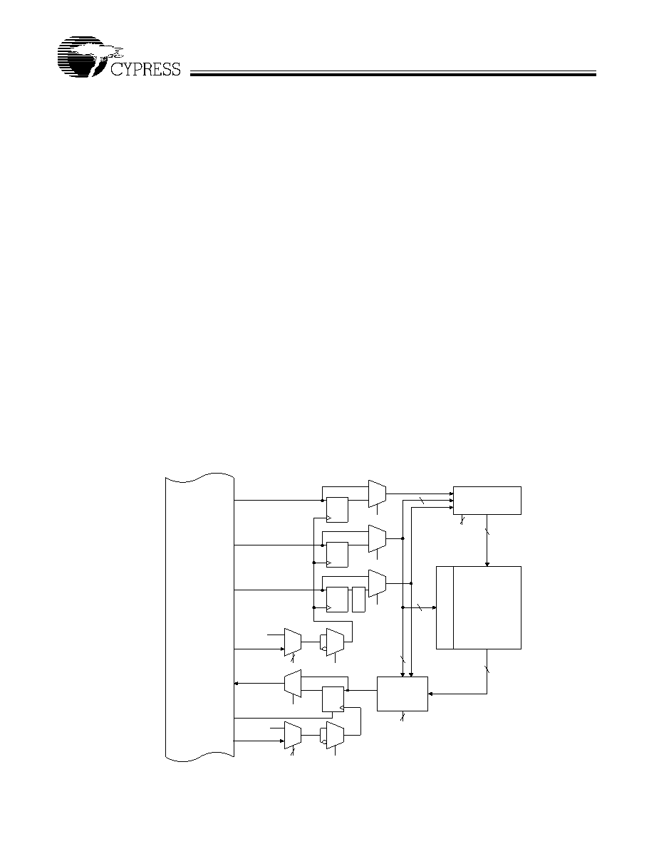
Cluster Memory
Each logic block cluster of the Delta39K contains two 8192-bit
cluster memory blocks. Figure 5 is a block diagram of the clus-
ter memory block and the interface of the cluster memory block
to the cluster PIM.
The output of the cluster memory block can be optionally reg-
istered to perform synchronous pipelining or to register asyn-
chronous read and write operations. The output registers con-
tain an asynchronous RESET which can be used in any type
of sequential logic circuits (e.g., state machines).
There are four global clocks (GCLK[3:0]) and one local clock
available for the input and the output registers. The local clock
for the input registers is independent of the one used for the
output registers. The local clock is generated in the user-de-
sign in a macrocell or comes from an I/O pin.
Cluster Memory Initialization
The cluster memory powers up in an undefined state, but is
set to a user-defined known state during configuration. To fa-
cilitate the use of look-up-table (LUT) logic and ROM applica-
tions, the cluster memory blocks can be initialized with a given
set of data when the device is configured at power up. For LUT
and ROM applications, the user cannot write to memory
blocks.
Channel Memory
The Delta39K architecture includes an embedded memory
block at each crossing point of horizontal and vertical routing
channels. The channel memory is a 4096-bit embedded mem-
ory block that can be configured as asynchronous or synchro-
nous Single-Port RAM, Dual-Port RAM, ROM, or synchronous
FIFO memory.
Data, address, and control inputs to the channel memory are
driven from horizontal and vertical routing channels. All data
and FIFO logic outputs drive dedicated tracks in the horizontal
and vertical routing channels. The clocks for the channel mem-
ory block are selected from four global clocks and pin inputs
from the horizontal and vertical channels. The clock muxes
also include a polarity mux for each clock so that the user can
choose an inverted clock.
Dual-Port (Channel Memory) Configuration
Each port has distinct address inputs, as well as separate data
and control inputs that can be accessed simultaneously. The
inputs to the Dual-Port memory are driven from the horizontal
and vertical routing channels. The data outputs drive dedicat-
ed tracks in the routing channels. The interface to the routing
is such that Port A of the Dual-Port interfaces primarily with the
horizontal routing channel and Port B interfaces primarily with
the vertical routing channel.
.
Figure 5. Block Diagram of Cluster Memory Block
5:1
DIN[7:0]
DQ
ADDR[12:0]
DQ
Cluster PIM
DQ
WE
Wr
it
e
Pu
ls
e
Write
Control
Logic
1024x8
Asynchronous
SRAM
Read
Control
Logic
Row
Dec
ode
(
1024
Rows
)
DOUT[7:0]
8
3
8
10
C
D
Q
GCLK[3:0]
5:1
R
RESET
GCLK[3:0]
C
Local CLK
2
Local CLK
3
2
3
C
相关PDF资料 |
PDF描述 |
|---|---|
| CY39050V256-222BBC | LOADABLE PLD, 7 ns, PBGA256 |
| CY39050V388-222MGC | LOADABLE PLD, 7 ns, PBGA388 |
| CY39050V484-222MBC | LOADABLE PLD, 7 ns, PBGA484 |
| CY39050Z208-222NC | LOADABLE PLD, 7 ns, PQFP208 |
| CY39050Z256-222BBC | LOADABLE PLD, 7 ns, PBGA256 |
相关代理商/技术参数 |
参数描述 |
|---|---|
| CY39050V208-233NTXC | 功能描述:IC CPLD 50K GATE 208BQFP RoHS:是 类别:集成电路 (IC) >> 嵌入式 - CPLD(复杂可编程逻辑器件) 系列:Delta 39K™ ISR™ 标准包装:24 系列:CoolRunner II 可编程类型:系统内可编程 最大延迟时间 tpd(1):7.1ns 电压电源 - 内部:1.7 V ~ 1.9 V 逻辑元件/逻辑块数目:24 宏单元数:384 门数:9000 输入/输出数:173 工作温度:0°C ~ 70°C 安装类型:表面贴装 封装/外壳:208-BFQFP 供应商设备封装:208-PQFP(28x28) 包装:托盘 |
| CY39050V208-83NTXC | 功能描述:IC CPLD 50K GATE 208BQFP RoHS:是 类别:集成电路 (IC) >> 嵌入式 - CPLD(复杂可编程逻辑器件) 系列:Delta 39K™ ISR™ 标准包装:24 系列:CoolRunner II 可编程类型:系统内可编程 最大延迟时间 tpd(1):7.1ns 电压电源 - 内部:1.7 V ~ 1.9 V 逻辑元件/逻辑块数目:24 宏单元数:384 门数:9000 输入/输出数:173 工作温度:0°C ~ 70°C 安装类型:表面贴装 封装/外壳:208-BFQFP 供应商设备封装:208-PQFP(28x28) 包装:托盘 |
| CY39050V208-83NTXI | 功能描述:IC CPLD 50K GATE 208BQFP RoHS:是 类别:集成电路 (IC) >> 嵌入式 - CPLD(复杂可编程逻辑器件) 系列:Delta 39K™ ISR™ 标准包装:24 系列:CoolRunner II 可编程类型:系统内可编程 最大延迟时间 tpd(1):7.1ns 电压电源 - 内部:1.7 V ~ 1.9 V 逻辑元件/逻辑块数目:24 宏单元数:384 门数:9000 输入/输出数:173 工作温度:0°C ~ 70°C 安装类型:表面贴装 封装/外壳:208-BFQFP 供应商设备封装:208-PQFP(28x28) 包装:托盘 |
| CY39050V484-125BBC | 制造商:CYPRESS 制造商全称:Cypress Semiconductor 功能描述:CPLDs at FPGA Densities |
| CY39050V484-125BBI | 制造商:CYPRESS 制造商全称:Cypress Semiconductor 功能描述:CPLDs at FPGA Densities |
发布紧急采购,3分钟左右您将得到回复。