- 您现在的位置:买卖IC网 > PDF目录170346 > CY39050V208-222NTC (CYPRESS SEMICONDUCTOR CORP) LOADABLE PLD, 7 ns, PQFP208 PDF资料下载
参数资料
| 型号: | CY39050V208-222NTC |
| 厂商: | CYPRESS SEMICONDUCTOR CORP |
| 元件分类: | PLD |
| 英文描述: | LOADABLE PLD, 7 ns, PQFP208 |
| 封装: | THERMALLY ENHANCED, QFP-208 |
| 文件页数: | 3/57页 |
| 文件大小: | 1166K |
| 代理商: | CY39050V208-222NTC |
第1页第2页当前第3页第4页第5页第6页第7页第8页第9页第10页第11页第12页第13页第14页第15页第16页第17页第18页第19页第20页第21页第22页第23页第24页第25页第26页第27页第28页第29页第30页第31页第32页第33页第34页第35页第36页第37页第38页第39页第40页第41页第42页第43页第44页第45页第46页第47页第48页第49页第50页第51页第52页第53页第54页第55页第56页第57页
PRELIMINARY
Delta39K ISR
CPLD Family
Document #: 38-03039 Rev. **
Page 11 of 57
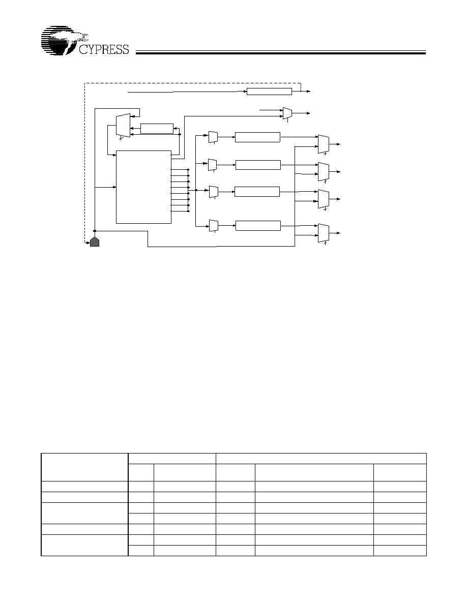
Spread Aware PLL
Each device in the Delta39K family features an on-chip PLL
designed using Spread Aware technology for low EMI applica-
tions. In general, PLLs are used to implement time-division-
multiplex circuits to achieve higher performance with fewer de-
vice resources.
For example, a system that operates on a 32-bit data path that
runs at 40 MHz can be implemented with 16-bit circuitry that
runs internally at 80 MHz. PLLs can also be used to take ad-
vantage of the positioning of the internally generated clock
edges to shift performance towards improved setup, hold or
clock-to-out times.
There are several frequency multiply (X1, X2, X4) and divide
(/1, /2, /3, /4, /5, /6. /8, /16) options available to create a wide
range of clock frequencies from a single clock input (GCLK[0]).
For increased flexibility, there are seven phase shifting options
which allow clock skew/de-skew by 45°, 90°, 135°, 180°, 225°,
270° or 315°.
The Voltage Controlled Oscillator (VCO), the core of the
Delta39K PLL is designed to operate within the frequency
range of 100 MHz to 266 MHz. Hence, the multiply option com-
bined with input (GCLK[0]) frequency should be selected such
that this VCO operating frequency requirement is met. This is
demonstrated in Table 2 (columns 1, 2, and 3).
Another feature of this PLL is the ability to drive the output
clock (INTCLK) off the Delta39K chip to clock other devices on
the board, as shown in Figure 9 above. This off-chip clock is
half the frequency of the output clock as it has to go through a
register (I/O register or a macrocell register).
This PLL can also be used for board de-skewing purpose by
driving a PLL output clock off-chip, routing it to the other de-
vices on the board and feeding it back to the PLL’s external
feedback input (GCLK[1]). When this feature is used, only lim-
ited multiply, divide and phase shift options can be used.
Table 2 describes the valid multiply and divide options that can
be used without an external feedback. Table 3 describes the
valid multiply & divide options that can be used with an exter-
nal feedback.
GCLK[3:0]
GCLK0
GCLK1
fb
Source
Clock
Clock Tree
Delay
Lock
PLL
X1, X2, X4
GCLK0
GCLK1
GCLK2
INTCLK0
INTCLK1
INTCLK2
Normal I/O signal path
Lock Detect/IO pin
Any Register
INTCLK0, INTCLK1, INTCLK2, INTCLK3
Send a global
clock off chip
C
Clk 00
Clk 900
Clk 1800
Clk 2700
Clk 2250
Clk 1350
Clk 450
Clk 3150
Divide
GCLK3
INTCLK3
2
fb
off-chip signal (external feedback)
Phase selection
÷ 1-6,8,16
Divide
÷ 1-6,8,16
Divide
÷ 1-6,8,16
Divide
÷ 1-6,8,16
Figure 9. Block Diagram of Spread Aware PLL
Table 2. PLL Multiply and Divide Options—without External Feedback
Input Frequency
(GCLK[0])
fPLLI (MHz)
Valid Multiply Options
Valid Divide Options
Value
VCO Output
Frequency (MHz)
Value
Output Frequency (INTCLK[3:0])
fPLLO (MHz)
Off-chip Clock
Frequency
25–33
4
100–133
1–6, 8, 16
6.25–133
3.12–66
33–50
4
133–200
1–6, 8, 16
8.33–200
4.16–100
50–66
4200–266
1–6, 8, 16
12.5–266
6.25–133
2100–133
1–6, 8, 16
6.25–133
3.12–66
66–100
2
133–200
1–6, 8, 16
8.3–200
4.16–100
100–133
2200–266
1–6, 8, 16
12.5–266
6.25–133
1100–133
1–6, 8, 16
6.25–133
3.12–66
相关PDF资料 |
PDF描述 |
|---|---|
| CY39050V256-222BBC | LOADABLE PLD, 7 ns, PBGA256 |
| CY39050V388-222MGC | LOADABLE PLD, 7 ns, PBGA388 |
| CY39050V484-222MBC | LOADABLE PLD, 7 ns, PBGA484 |
| CY39050Z208-222NC | LOADABLE PLD, 7 ns, PQFP208 |
| CY39050Z256-222BBC | LOADABLE PLD, 7 ns, PBGA256 |
相关代理商/技术参数 |
参数描述 |
|---|---|
| CY39050V208-233NTXC | 功能描述:IC CPLD 50K GATE 208BQFP RoHS:是 类别:集成电路 (IC) >> 嵌入式 - CPLD(复杂可编程逻辑器件) 系列:Delta 39K™ ISR™ 标准包装:24 系列:CoolRunner II 可编程类型:系统内可编程 最大延迟时间 tpd(1):7.1ns 电压电源 - 内部:1.7 V ~ 1.9 V 逻辑元件/逻辑块数目:24 宏单元数:384 门数:9000 输入/输出数:173 工作温度:0°C ~ 70°C 安装类型:表面贴装 封装/外壳:208-BFQFP 供应商设备封装:208-PQFP(28x28) 包装:托盘 |
| CY39050V208-83NTXC | 功能描述:IC CPLD 50K GATE 208BQFP RoHS:是 类别:集成电路 (IC) >> 嵌入式 - CPLD(复杂可编程逻辑器件) 系列:Delta 39K™ ISR™ 标准包装:24 系列:CoolRunner II 可编程类型:系统内可编程 最大延迟时间 tpd(1):7.1ns 电压电源 - 内部:1.7 V ~ 1.9 V 逻辑元件/逻辑块数目:24 宏单元数:384 门数:9000 输入/输出数:173 工作温度:0°C ~ 70°C 安装类型:表面贴装 封装/外壳:208-BFQFP 供应商设备封装:208-PQFP(28x28) 包装:托盘 |
| CY39050V208-83NTXI | 功能描述:IC CPLD 50K GATE 208BQFP RoHS:是 类别:集成电路 (IC) >> 嵌入式 - CPLD(复杂可编程逻辑器件) 系列:Delta 39K™ ISR™ 标准包装:24 系列:CoolRunner II 可编程类型:系统内可编程 最大延迟时间 tpd(1):7.1ns 电压电源 - 内部:1.7 V ~ 1.9 V 逻辑元件/逻辑块数目:24 宏单元数:384 门数:9000 输入/输出数:173 工作温度:0°C ~ 70°C 安装类型:表面贴装 封装/外壳:208-BFQFP 供应商设备封装:208-PQFP(28x28) 包装:托盘 |
| CY39050V484-125BBC | 制造商:CYPRESS 制造商全称:Cypress Semiconductor 功能描述:CPLDs at FPGA Densities |
| CY39050V484-125BBI | 制造商:CYPRESS 制造商全称:Cypress Semiconductor 功能描述:CPLDs at FPGA Densities |
发布紧急采购,3分钟左右您将得到回复。