- 您现在的位置:买卖IC网 > PDF目录170346 > CY39050V208-222NTC (CYPRESS SEMICONDUCTOR CORP) LOADABLE PLD, 7 ns, PQFP208 PDF资料下载
参数资料
| 型号: | CY39050V208-222NTC |
| 厂商: | CYPRESS SEMICONDUCTOR CORP |
| 元件分类: | PLD |
| 英文描述: | LOADABLE PLD, 7 ns, PQFP208 |
| 封装: | THERMALLY ENHANCED, QFP-208 |
| 文件页数: | 57/57页 |
| 文件大小: | 1166K |
| 代理商: | CY39050V208-222NTC |
第1页第2页第3页第4页第5页第6页第7页第8页第9页第10页第11页第12页第13页第14页第15页第16页第17页第18页第19页第20页第21页第22页第23页第24页第25页第26页第27页第28页第29页第30页第31页第32页第33页第34页第35页第36页第37页第38页第39页第40页第41页第42页第43页第44页第45页第46页第47页第48页第49页第50页第51页第52页第53页第54页第55页第56页当前第57页
PRELIMINARY
Delta39K ISR
CPLD Family
Document #: 38-03039 Rev. **
Page 9 of 57
Channel Memory Initialization
The channel memory powers up in an undefined state, but is
set to a user-defined known state during configuration. To fa-
cilitate the use of look-up-table (LUT) logic and ROM applica-
tions, the channel memory blocks can be initialized with a giv-
en set of data when the device is configured at power up. For
LUT and ROM applications, the user cannot write to memory
blocks.
Channel Memory Routing Interface
Similar to LBC outputs, the channel memory blocks feature
dedicated tracks in the horizontal and vertical routing channels
for the data outputs and the flag outputs, as shown in
Figure 6. This allows the channel memory blocks to be ex-
panded easily. These dedicated lines can be routed to I/O pins
as chip outputs or to other logic block clusters to be used in
logic equations.
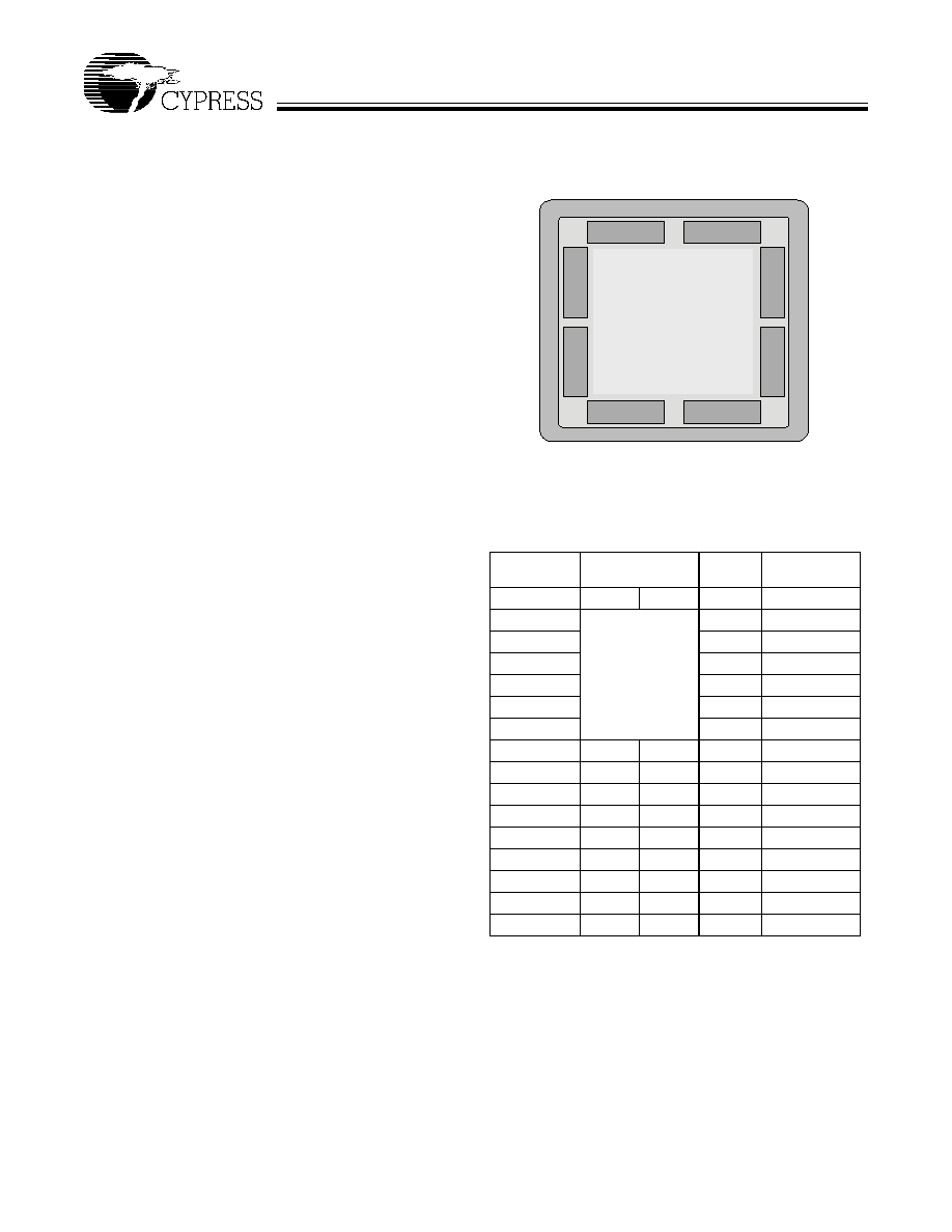
I/O Banks
The Delta39K interfaces the horizontal and vertical routing
channels to the pins through I/O banks. There are 8 I/O banks
per device as shown in Figure 7, and all I/Os from an I/O bank
are located in the same section of a package for PCB layout
convenience.
For each package type, Delta39K devices of different densities
keep given pins in the same I/O banks. This supports and sim-
plifies design migration across densities.
Each I/O bank contains several I/O cells, and each I/O cell
contains an input/output register, an output enable register,
programmable slew rate control and programmable bus hold
control logic. Each I/O cell drives a pin output of the device;
the cell also supplies an input to the device that connects to a
dedicated track in the associated routing channel.
There are four dedicated inputs (GCTl[3:0]) that are used as
Global Control Signals available to every I/O cell. These global
control signals may be used as output enables, register resets
and register clock enables as shown in Figure 8.
Each I/O bank can use any supported I/O standard by supply-
ing appropriate VREF and VCCIO voltages. All the VREF and
VCCIO pins in an I/O bank must be connected to the same VREF
and VCCIO voltage respectively. This requirement restricts the
number of I/O standards supported by an I/O bank at any given
time.
The number of I/Os which can be used in each I/O bank de-
pend on the type of I/O standards and the number of VCCIO
and GND pins being used. This restriction is derived from the
electromigration limit of the VCCIO and GND bussing on the
chip. Please refer to the note on page 17 and the application
note titled “Delta39K Family Device I/O Standards and Config-
urations” for details.
Figure 7. Delta39K I/O Bank Block Diagram
I/O Standards
I/O
Standard
VREF (V)
VCCIO
Termination
Voltage (VTT)
Min.
Max.
LVTTL
N/A
3.3V
N/A
LVCMOS
3.3V
N/A
LVCMOS3
3.0V
N/A
LVCMOS2
2.5V
N/A
LVCMOS18
1.8V
N/A
3.3V PCI
3.3V
N/A
GTL+
0.9
1.1
N/A
1.5
SSTL3 I
1.3
1.7
3.3V
1.5
SSTL3 II
1.3
1.7
3.3V
1.5
SSTL2 I
1.15
1.35
2.5V
1.25
SSTL2 II
1.15
1.35
2.5V
1.25
HSTL I
0.68
0.9
1.5V
0.75
HSTL II
0.68
0.9
1.5V
0.75
HSTL III
0.68
0.9
1.5V
1.5
HSTL IV
0.68
0.9
1.5V
1.5
Delta39K
bank
0
bank
1
bank
4
bank
5
bank 2
bank 3
bank 6
bank 7
Delta39K
相关PDF资料 |
PDF描述 |
|---|---|
| CY39050V256-222BBC | LOADABLE PLD, 7 ns, PBGA256 |
| CY39050V388-222MGC | LOADABLE PLD, 7 ns, PBGA388 |
| CY39050V484-222MBC | LOADABLE PLD, 7 ns, PBGA484 |
| CY39050Z208-222NC | LOADABLE PLD, 7 ns, PQFP208 |
| CY39050Z256-222BBC | LOADABLE PLD, 7 ns, PBGA256 |
相关代理商/技术参数 |
参数描述 |
|---|---|
| CY39050V208-233NTXC | 功能描述:IC CPLD 50K GATE 208BQFP RoHS:是 类别:集成电路 (IC) >> 嵌入式 - CPLD(复杂可编程逻辑器件) 系列:Delta 39K™ ISR™ 标准包装:24 系列:CoolRunner II 可编程类型:系统内可编程 最大延迟时间 tpd(1):7.1ns 电压电源 - 内部:1.7 V ~ 1.9 V 逻辑元件/逻辑块数目:24 宏单元数:384 门数:9000 输入/输出数:173 工作温度:0°C ~ 70°C 安装类型:表面贴装 封装/外壳:208-BFQFP 供应商设备封装:208-PQFP(28x28) 包装:托盘 |
| CY39050V208-83NTXC | 功能描述:IC CPLD 50K GATE 208BQFP RoHS:是 类别:集成电路 (IC) >> 嵌入式 - CPLD(复杂可编程逻辑器件) 系列:Delta 39K™ ISR™ 标准包装:24 系列:CoolRunner II 可编程类型:系统内可编程 最大延迟时间 tpd(1):7.1ns 电压电源 - 内部:1.7 V ~ 1.9 V 逻辑元件/逻辑块数目:24 宏单元数:384 门数:9000 输入/输出数:173 工作温度:0°C ~ 70°C 安装类型:表面贴装 封装/外壳:208-BFQFP 供应商设备封装:208-PQFP(28x28) 包装:托盘 |
| CY39050V208-83NTXI | 功能描述:IC CPLD 50K GATE 208BQFP RoHS:是 类别:集成电路 (IC) >> 嵌入式 - CPLD(复杂可编程逻辑器件) 系列:Delta 39K™ ISR™ 标准包装:24 系列:CoolRunner II 可编程类型:系统内可编程 最大延迟时间 tpd(1):7.1ns 电压电源 - 内部:1.7 V ~ 1.9 V 逻辑元件/逻辑块数目:24 宏单元数:384 门数:9000 输入/输出数:173 工作温度:0°C ~ 70°C 安装类型:表面贴装 封装/外壳:208-BFQFP 供应商设备封装:208-PQFP(28x28) 包装:托盘 |
| CY39050V484-125BBC | 制造商:CYPRESS 制造商全称:Cypress Semiconductor 功能描述:CPLDs at FPGA Densities |
| CY39050V484-125BBI | 制造商:CYPRESS 制造商全称:Cypress Semiconductor 功能描述:CPLDs at FPGA Densities |
发布紧急采购,3分钟左右您将得到回复。