- 您现在的位置:买卖IC网 > PDF目录170346 > CY39050V208-222NTC (CYPRESS SEMICONDUCTOR CORP) LOADABLE PLD, 7 ns, PQFP208 PDF资料下载
参数资料
| 型号: | CY39050V208-222NTC |
| 厂商: | CYPRESS SEMICONDUCTOR CORP |
| 元件分类: | PLD |
| 英文描述: | LOADABLE PLD, 7 ns, PQFP208 |
| 封装: | THERMALLY ENHANCED, QFP-208 |
| 文件页数: | 34/57页 |
| 文件大小: | 1166K |
| 代理商: | CY39050V208-222NTC |
第1页第2页第3页第4页第5页第6页第7页第8页第9页第10页第11页第12页第13页第14页第15页第16页第17页第18页第19页第20页第21页第22页第23页第24页第25页第26页第27页第28页第29页第30页第31页第32页第33页当前第34页第35页第36页第37页第38页第39页第40页第41页第42页第43页第44页第45页第46页第47页第48页第49页第50页第51页第52页第53页第54页第55页第56页第57页
PRELIMINARY
Delta39K ISR
CPLD Family
Document #: 38-03039 Rev. **
Page 4 of 57
General Description
The Delta39K family, based on a 0.18
m, 6-layer metal
CMOS logic process, offers a wide range of high-density solu-
tions at unparalleled system performance. The Delta39K fam-
ily is designed to combine the high speed, predictable timing,
and ease of use of CPLDs with the high densities and low
power of FPGAs. With devices ranging from 15,000 to 350,000
usable gates, the family features devices ten times the size of
previously available CPLDs. Even at these large densities, the
Delta39K family is fast enough to implement a fully synthesiz-
able 64-bit, 66-MHz PCI core.
The architecture is based on Logic Block Clusters (LBC) that
are connected by Horizontal and Vertical (H&V) routing chan-
nels. Each LBC features eight individual Logic Blocks (LB) and
two cluster memory blocks. Adjacent to each LBC is a channel
memory block, which can be accessed directly from the I/O
pins. Both types of memory blocks are highly configurable and
can be cascaded in width and depth. See Figure 1 for a block
diagram of the Delta39K architecture.
All the members of the Delta39K family have Cypress’s highly
regarded In-System Reprogrammability (ISR) feature, which
simplifies both design and manufacturing flows, thereby re-
ducing costs. The ISR feature provides the ability to reconfig-
ure the devices without having design changes cause pinout
or timing changes in most cases. The Cypress ISR function is
implemented through a JTAG-compliant serial interface. Data
is shifted in and out through the TDI and TDO pins respective-
ly. Superior routability, simple timing, and the ISR allows users
to change existing logic designs while simultaneously fixing
pinout assignments and maintaining system performance.
The entire family features JTAG for ISR and boundary scan,
and is compatible with the PCI Local Bus specification, meet-
ing the electrical and timing requirements. The Delta39K fam-
ily also features user programmable bus-hold and slew rate
control capabilities on each I/O pin.
AnyVolt Interface
All Delta39KV devices feature an on-chip regulator, which ac-
cepts 3.3V or 2.5V on the VCC supply pins and steps it down
to 1.8V internally, the voltage level at which the core operates.
The Delta39KZ devices accept 1.8V on the VCC supply pins
directly. With Delta39K’s AnyVolt technology, the I/O pins can
be connected to either 1.8V, 2.5V, or 3.3V. All Delta39K devic-
es are 3.3V tolerant regardless of VCCIO or VCC settings.
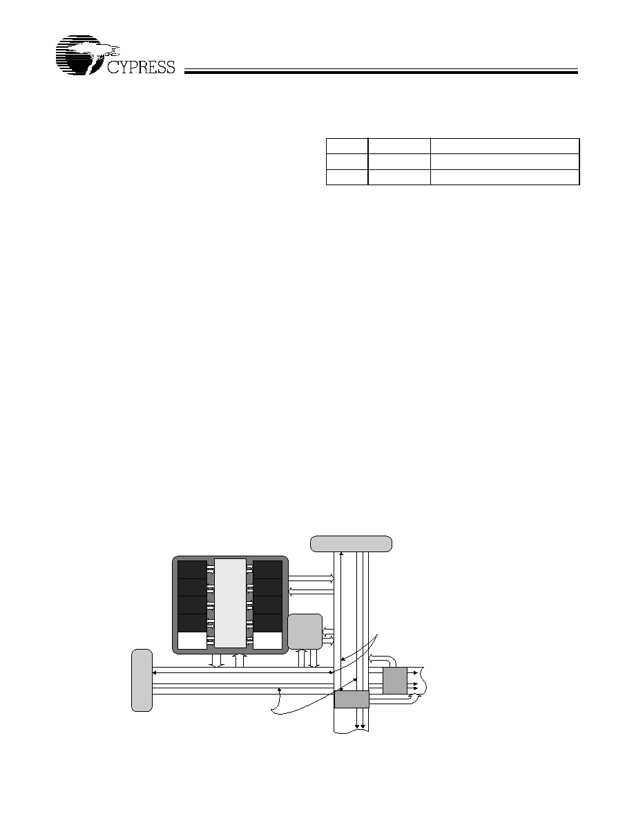
Global Routing Description
The routing architecture of the Delta39K is made up of hori-
zontal and vertical (H&V) routing channels. These routing
channels allow signals from each of the Delta39K architectural
components to communicate with one another. In addition to
the horizontal and vertical routing channels that interconnect
the I/O banks, channel memory blocks, and logic block clus-
ters, each LBC contains a Programmable Interconnect Matrix
(PIM), which is used to route signals among the logic blocks
and the cluster memory blocks.
Figure 2 is a block diagram of the routing channels that inter-
face within the Delta39K architecture. The LBC is exactly the
same for every member of the Delta39K CPLD family.
Logic Block Cluster (LBC)
The Delta39K architecture consists of several logic block clus-
ters, each of which have 8 Logic Blocks (LB) and 2 cluster
memory blocks connected via a Programmable Interconnect
Matrix (PIM) as shown in Figure 3. Each cluster memory block
consists of 8-Kbit single-port RAM, which is configurable as
synchronous or asynchronous. The cluster memory blocks
can be cascaded with other cluster memory blocks within the
same LBC as well as other LBCs to implement larger memory
functions. If a cluster memory block is not specifically utilized
by the designer, Cypress’s Warp software can automatically
use it to implement large blocks of logic.
All LBCs interface with each other via horizontal and vertical
routing channels.
Note:
5.
For HSTL only.
Device
VCC
VCCIO
39KV
3.3V or 2.5V
3.3V or 2.5V or 1.8V or 1.5V[5]
39KZ
1.8V
3.3V or 2.5V or 1.8V or 1.5V[5]
Figure 2. Delta39K Routing Interface
LB
Cluster
PIM
Cluster
Memory
Block
LB
Cluster
Memory
Block
LB
Channel
Memory
Block
I/O Block
I/O
B
lock
Channel memory
outputs drive
dedicated tracks in the
horizontal and vertical
routing channels
H-to-V
PIM
V-to-H
PIM
Pin inputs from the I/O cells
drive dedicated tracks in the
horizontal and vertical routing
channels
72
64
相关PDF资料 |
PDF描述 |
|---|---|
| CY39050V256-222BBC | LOADABLE PLD, 7 ns, PBGA256 |
| CY39050V388-222MGC | LOADABLE PLD, 7 ns, PBGA388 |
| CY39050V484-222MBC | LOADABLE PLD, 7 ns, PBGA484 |
| CY39050Z208-222NC | LOADABLE PLD, 7 ns, PQFP208 |
| CY39050Z256-222BBC | LOADABLE PLD, 7 ns, PBGA256 |
相关代理商/技术参数 |
参数描述 |
|---|---|
| CY39050V208-233NTXC | 功能描述:IC CPLD 50K GATE 208BQFP RoHS:是 类别:集成电路 (IC) >> 嵌入式 - CPLD(复杂可编程逻辑器件) 系列:Delta 39K™ ISR™ 标准包装:24 系列:CoolRunner II 可编程类型:系统内可编程 最大延迟时间 tpd(1):7.1ns 电压电源 - 内部:1.7 V ~ 1.9 V 逻辑元件/逻辑块数目:24 宏单元数:384 门数:9000 输入/输出数:173 工作温度:0°C ~ 70°C 安装类型:表面贴装 封装/外壳:208-BFQFP 供应商设备封装:208-PQFP(28x28) 包装:托盘 |
| CY39050V208-83NTXC | 功能描述:IC CPLD 50K GATE 208BQFP RoHS:是 类别:集成电路 (IC) >> 嵌入式 - CPLD(复杂可编程逻辑器件) 系列:Delta 39K™ ISR™ 标准包装:24 系列:CoolRunner II 可编程类型:系统内可编程 最大延迟时间 tpd(1):7.1ns 电压电源 - 内部:1.7 V ~ 1.9 V 逻辑元件/逻辑块数目:24 宏单元数:384 门数:9000 输入/输出数:173 工作温度:0°C ~ 70°C 安装类型:表面贴装 封装/外壳:208-BFQFP 供应商设备封装:208-PQFP(28x28) 包装:托盘 |
| CY39050V208-83NTXI | 功能描述:IC CPLD 50K GATE 208BQFP RoHS:是 类别:集成电路 (IC) >> 嵌入式 - CPLD(复杂可编程逻辑器件) 系列:Delta 39K™ ISR™ 标准包装:24 系列:CoolRunner II 可编程类型:系统内可编程 最大延迟时间 tpd(1):7.1ns 电压电源 - 内部:1.7 V ~ 1.9 V 逻辑元件/逻辑块数目:24 宏单元数:384 门数:9000 输入/输出数:173 工作温度:0°C ~ 70°C 安装类型:表面贴装 封装/外壳:208-BFQFP 供应商设备封装:208-PQFP(28x28) 包装:托盘 |
| CY39050V484-125BBC | 制造商:CYPRESS 制造商全称:Cypress Semiconductor 功能描述:CPLDs at FPGA Densities |
| CY39050V484-125BBI | 制造商:CYPRESS 制造商全称:Cypress Semiconductor 功能描述:CPLDs at FPGA Densities |
发布紧急采购,3分钟左右您将得到回复。