- 您现在的位置:买卖IC网 > PDF目录295374 > CY7C1177V18-333BZXC (CYPRESS SEMICONDUCTOR CORP) 18-Mbit DDR-II+ SRAM 2-Word Burst Architecture (2.5 Cycle Read Latency) PDF资料下载
参数资料
| 型号: | CY7C1177V18-333BZXC |
| 厂商: | CYPRESS SEMICONDUCTOR CORP |
| 元件分类: | SRAM |
| 英文描述: | 18-Mbit DDR-II+ SRAM 2-Word Burst Architecture (2.5 Cycle Read Latency) |
| 中文描述: | 2M X 9 DDR SRAM, 0.45 ns, PBGA165 |
| 封装: | 13 X 15 MM, 1.40 MM HEIGHT, LEAD FREE, MO-216, FBGA-165 |
| 文件页数: | 20/27页 |
| 文件大小: | 648K |
| 代理商: | CY7C1177V18-333BZXC |
第1页第2页第3页第4页第5页第6页第7页第8页第9页第10页第11页第12页第13页第14页第15页第16页第17页第18页第19页当前第20页第21页第22页第23页第24页第25页第26页第27页
Document Number: 001-06620 Rev. *D
Revised March 06, 2008
Page 27 of 27
QDR is a trademark of Cypress Semiconductor Corp. QDR RAMs and Quad Data Rate RAMs comprise a new family of products developed by Cypress, IDT, NEC, Renesas, and Samsung. All
product and company names mentioned in this document are the trademarks of their respective holders.
CY7C1166V18, CY7C1177V18
CY7C1168V18, CY7C1170V18
Cypress Semiconductor Corporation, 2006-2008. The information contained herein is subject to change without notice. Cypress Semiconductor Corporation assumes no responsibility for the use of
any circuitry other than circuitry embodied in a Cypress product. Nor does it convey or imply any license under patent or other rights. Cypress products are not warranted nor intended to be used for
medical, life support, life saving, critical control or safety applications, unless pursuant to an express written agreement with Cypress. Furthermore, Cypress does not authorize its products for use as
critical components in life-support systems where a malfunction or failure may reasonably be expected to result in significant injury to the user. The inclusion of Cypress products in life-support systems
application implies that the manufacturer assumes all risk of such use and in doing so indemnifies Cypress against all charges.
Any Source Code (software and/or firmware) is owned by Cypress Semiconductor Corporation (Cypress) and is protected by and subject to worldwide patent protection (United States and foreign),
United States copyright laws and international treaty provisions. Cypress hereby grants to licensee a personal, non-exclusive, non-transferable license to copy, use, modify, create derivative works of,
and compile the Cypress Source Code and derivative works for the sole purpose of creating custom software and or firmware in support of licensee product to be used only in conjunction with a Cypress
integrated circuit as specified in the applicable agreement. Any reproduction, modification, translation, compilation, or representation of this Source Code except as specified above is prohibited without
the express written permission of Cypress.
Disclaimer: CYPRESS MAKES NO WARRANTY OF ANY KIND, EXPRESS OR IMPLIED, WITH REGARD TO THIS MATERIAL, INCLUDING, BUT NOT LIMITED TO, THE IMPLIED WARRANTIES
OF MERCHANTABILITY AND FITNESS FOR A PARTICULAR PURPOSE. Cypress reserves the right to make changes without further notice to the materials described herein. Cypress does not
assume any liability arising out of the application or use of any product or circuit described herein. Cypress does not authorize its products for use as critical components in life-support systems where
a malfunction or failure may reasonably be expected to result in significant injury to the user. The inclusion of Cypress’ product in a life-support systems application implies that the manufacturer
assumes all risk of such use and in doing so indemnifies Cypress against all charges.
Use may be limited by and subject to the applicable Cypress software license agreement.
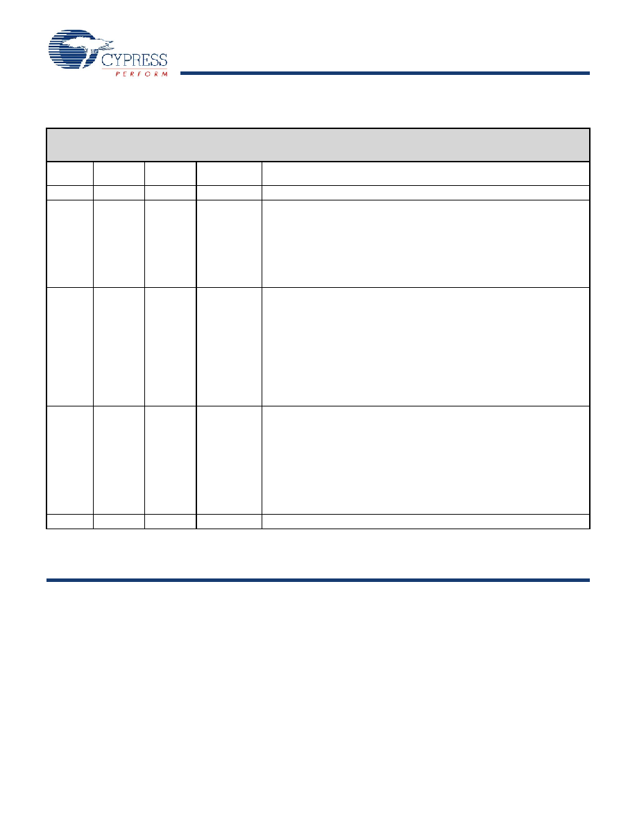
Document History Page
Document Title: CY7C1166V18/CY7C1177V18/CY7C1168V18/CY7C1170V18, 18-Mbit DDR-II+ SRAM 2-Word Burst
Architecture (2.5 Cycle Read Latency)
Document Number: 001-06620
REV.
ECN No.
Issue Date
Orig. of
Change
Description of Change
**
430351
See ECN
NXR
New data sheet
*A
461654
See ECN
NXR
Revised the MPNs from
CY7C1177BV18 to CY7C1166V18
CY7C1168BV18 to CY7C1177V18
CY7C1170BV18 to CY7C1168V18
Changed tTH and tTL from 40 ns to 20 ns, changed tTMSS, tTDIS, tCS, tTMSH, tTDIH,
tCH from 10 ns to 5 ns and changed tTDOV from 20 ns to 10 ns in TAP AC
Switching Characteristics table
Modified Power Up waveform
*B
497629
See ECN
NXR
Changed the VDDQ operating voltage to 1.4V to VDD in the Features section, in
Operating Range table and in the DC Electrical Characteristics table
Added foot note in page 1
Changed the Maximum rating of Ambient Temperature with Power Applied from
–10°C to +85°C to –55°C to +125°C
Changed VREF (max) spec from 0.85V to 0.95V in the DC Electrical Character-
istics table and in the note below the table
Updated foot note 21 to specify Overshoot and Undershoot Spec
Updated
Θ
JA and ΘJC values
Removed x9 part and its related information
Updated foot note 24
*C
1175245
See ECN
VKN/KKVTMP Converted from preliminary to final
Added x8 and x9 parts
Updated logic block diagram for x18 and x36 parts
Changed IDD values from 830 mA to 1080 mA for 400 MHz, 794 mA to 1020 mA
for 375 MHz, 733 mA to 920 mA for 333 MHz, 685 mA to 850 mA for 300 MHz
Changed ISB values from 235 mA to 300 mA for 400 MHz, 227 mA to 290 mA
for 375 MHz, 212 mA to 260 mA for 333 MHz, 201 mA to 250 mA for 300 MHz
Changed tCYC(max) spec to 8.4 ns for all speed bins
Changed
Θ
JA value from 13.48 °C/W to 17.2 °C/W
Updated Ordering Information table
*D
2199066
See ECN
VKN/AESA
Added footnote# 19 related to IDD
相关PDF资料 |
PDF描述 |
|---|---|
| CY7C1177V18-333BZXI | 18-Mbit DDR-II+ SRAM 2-Word Burst Architecture (2.5 Cycle Read Latency) |
| CY7C1170V18 | 18-Mbit DDR-II+ SRAM 2-Word Burst Architecture (2.5 Cycle Read Latency) |
| CY7C1177V18 | 18-Mbit DDR-II+ SRAM 2-Word Burst Architecture (2.5 Cycle Read Latency) |
| CY7C1215H-100AXC | 1-Mbit (32K x 32) Pipelined Sync SRAM |
| CY7C1215H-100AXI | 1-Mbit (32K x 32) Pipelined Sync SRAM |
相关代理商/技术参数 |
参数描述 |
|---|---|
| CY7C1214F-100AC | 制造商:Cypress Semiconductor 功能描述: |
| CY7C1214F-100ACT | 制造商:Cypress Semiconductor 功能描述: |
| CY7C1215F-166AC | 制造商:Rochester Electronics LLC 功能描述:1MB (32K X 32) 3.3V PIPELINE SCD - Bulk 制造商:Cypress Semiconductor 功能描述: |
| CY7C1215H-166AXC | 制造商:Cypress Semiconductor 功能描述:SRAM SYNC SGL 3.3V 1MBIT 32KX32 3.5NS 100TQFP - Bulk |
| CY7C1217H-133AXC | 制造商:Cypress Semiconductor 功能描述:SRAM SYNC QUAD 3.3V 1.125MBIT 32KX36 7.5NS 100TQFP - Bulk |
发布紧急采购,3分钟左右您将得到回复。