- 您现在的位置:买卖IC网 > PDF目录295374 > CY7C1177V18-333BZXC (CYPRESS SEMICONDUCTOR CORP) 18-Mbit DDR-II+ SRAM 2-Word Burst Architecture (2.5 Cycle Read Latency) PDF资料下载
参数资料
| 型号: | CY7C1177V18-333BZXC |
| 厂商: | CYPRESS SEMICONDUCTOR CORP |
| 元件分类: | SRAM |
| 英文描述: | 18-Mbit DDR-II+ SRAM 2-Word Burst Architecture (2.5 Cycle Read Latency) |
| 中文描述: | 2M X 9 DDR SRAM, 0.45 ns, PBGA165 |
| 封装: | 13 X 15 MM, 1.40 MM HEIGHT, LEAD FREE, MO-216, FBGA-165 |
| 文件页数: | 27/27页 |
| 文件大小: | 648K |
| 代理商: | CY7C1177V18-333BZXC |
第1页第2页第3页第4页第5页第6页第7页第8页第9页第10页第11页第12页第13页第14页第15页第16页第17页第18页第19页第20页第21页第22页第23页第24页第25页第26页当前第27页
CY7C1166V18, CY7C1177V18
CY7C1168V18, CY7C1170V18
Document Number: 001-06620 Rev. *D
Page 9 of 27
echo clock and follows the timing of any data pin. This signal is
asserted half a cycle before valid data arrives.
DLL
These chips use a Delay Lock Loop (DLL) that is designed to
function between 120 MHz and the specified maximum clock
frequency. The DLL may be disabled by applying ground to the
DOFF pin. When the DLL is turned off, the device behaves in
DDR-I mode (with 1.0 cycle latency and a longer access time).
For more information, refer to the application note, “DLL Consid-
erations in QDRII/DDRII/QDRII+/DDRII+”. The DLL can also be
reset by slowing or stopping the input clocks K and K for a
minimum of 30 ns. However, it is not necessary for the DLL to be
reset to lock to the desired frequency. During power up, when the
DOFF is tied HIGH, the DLL gets locked after 2048 cycles of
stable clock.
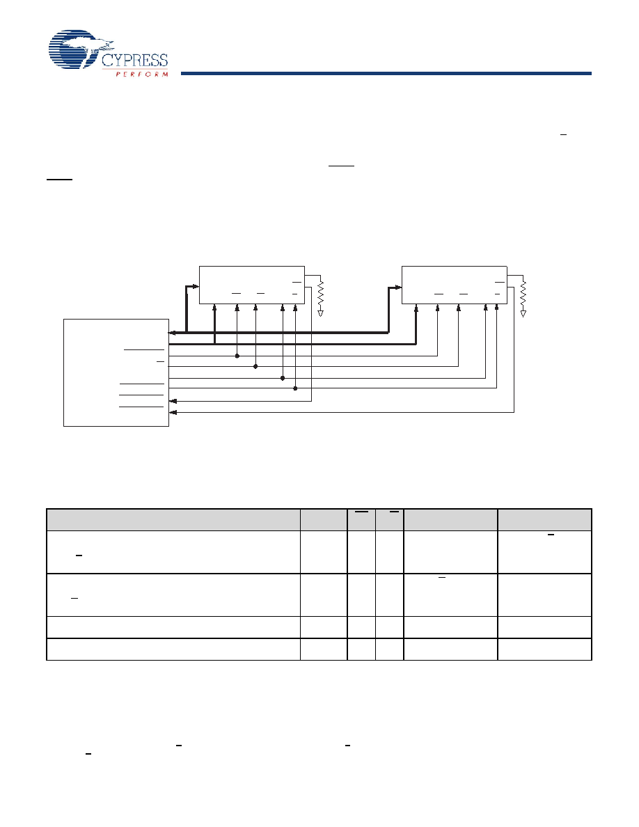
Application Example
Figure 1 shows two DDR-II+ used in an application.
Figure 1. Application Example
Truth Table
The truth table for the CY7C1166V18, CY7C1177V18, CY7C1168V18, and CY7C1170V18 follows. [2, 3, 4, 5, 6, 7]
Operation
K
LD
R/W
DQ
Write Cycle:
Load address; wait one cycle; input write data on consecutive
K and K rising edges.
L-H
L
D(A) at K (t + 1)
↑
D(A + 1) at K (t + 1)
↑
Read Cycle: (2.5 Cycle Latency)
Load address; wait two and a half cycle; read data on consec-
utive K and K rising edges.
L-H
L
H
Q(A) at K (t + 2)
↑
Q(A + 1) at K (t + 3)
↑
NOP: No Operation
L-H
H
X
High-Z
Standby: Clock Stopped
Stopped
X
Previous State
BUS
MASTER
(CPU or ASIC)
DQ
Addresses
Cycle Start
R/W
Source CLK
Echo Clock1/Echo Clock1
Echo Clock2/Echo Clock2
R = 250ohms
LD
R/W
DQ
A
SRAM#1
K
ZQ
CQ/CQ
K
R = 250ohms
LD
R/W
DQ
A
SRAM#2
K
ZQ
CQ/CQ
K
Notes
2. X = “Don’t Care,” H = Logic HIGH, L = Logic LOW,
↑ represents rising edge.
3. Device powers up deselected and the outputs in a tri-state condition.
4. “A” represents address location latched by the devices when transaction was initiated and A + 1 represents the addresses sequence in the burst.
5. “t” represents the cycle at which a Read/Write operation is started. t + 1, t + 2, and t + 3 are the first, second, and third clock cycles succeeding the “t” clock cycle.
6. Data inputs are registered at K and K rising edges. Data outputs are delivered on K and K rising edges.
7. Do K = K = HIGH when clock is stopped. This is not essential, but permits most rapid restart by overcoming transmission line charging symmetrically.
相关PDF资料 |
PDF描述 |
|---|---|
| CY7C1177V18-333BZXI | 18-Mbit DDR-II+ SRAM 2-Word Burst Architecture (2.5 Cycle Read Latency) |
| CY7C1170V18 | 18-Mbit DDR-II+ SRAM 2-Word Burst Architecture (2.5 Cycle Read Latency) |
| CY7C1177V18 | 18-Mbit DDR-II+ SRAM 2-Word Burst Architecture (2.5 Cycle Read Latency) |
| CY7C1215H-100AXC | 1-Mbit (32K x 32) Pipelined Sync SRAM |
| CY7C1215H-100AXI | 1-Mbit (32K x 32) Pipelined Sync SRAM |
相关代理商/技术参数 |
参数描述 |
|---|---|
| CY7C1214F-100AC | 制造商:Cypress Semiconductor 功能描述: |
| CY7C1214F-100ACT | 制造商:Cypress Semiconductor 功能描述: |
| CY7C1215F-166AC | 制造商:Rochester Electronics LLC 功能描述:1MB (32K X 32) 3.3V PIPELINE SCD - Bulk 制造商:Cypress Semiconductor 功能描述: |
| CY7C1215H-166AXC | 制造商:Cypress Semiconductor 功能描述:SRAM SYNC SGL 3.3V 1MBIT 32KX32 3.5NS 100TQFP - Bulk |
| CY7C1217H-133AXC | 制造商:Cypress Semiconductor 功能描述:SRAM SYNC QUAD 3.3V 1.125MBIT 32KX36 7.5NS 100TQFP - Bulk |
发布紧急采购,3分钟左右您将得到回复。