- 您现在的位置:买卖IC网 > PDF目录16615 > DC859A (Linear Technology)EVAL BOARD FOR LTC4267 PDF资料下载
参数资料
| 型号: | DC859A |
| 厂商: | Linear Technology |
| 文件页数: | 17/32页 |
| 文件大小: | 0K |
| 描述: | EVAL BOARD FOR LTC4267 |
| 设计资源: | DC859A Design File DC859A Schematic |
| 标准包装: | 1 |
| 主要目的: | 电源管理,以太网供电(POE) |
| 嵌入式: | 否 |
| 已用 IC / 零件: | LTC4267 |
| 已供物品: | 板 |
第1页第2页第3页第4页第5页第6页第7页第8页第9页第10页第11页第12页第13页第14页第15页第16页当前第17页第18页第19页第20页第21页第22页第23页第24页第25页第26页第27页第28页第29页第30页第31页第32页
LTC4267
24
4267fc
Selecting the Switching Transistor
With the N-channel power MOSFET driving the primary of
the transformer, the inductance will cause the drain of the
MOSFET to traverse twice the voltage across VPORTP and
PGND. The LTC4267 operates with a maximum supply of
– 57V; thus the MOSFET must be rated to handle 114V or
more with sufcient design margin. Typical transistors have
150V ratings while some manufacturers have developed
120V rated MOSFETs specically for Power-over-Ethernet
applications.
The NGATE pin of the LTC4267 drives the gate of the
N-channel MOSFET. NGATE will traverse a rail-to-rail volt-
age from PGND to PVCC. The designer must ensure the
MOSFET provides a low “ON” resistance when switched
to PVCC as well as ensure the gate of the MOSFET can
handle the PVCC supply voltage.
For high efciency applications, select an N-channel
MOSFET with low total gate charge. The lower total gate
charge improves the efciency of the NGATE drive circuit
and minimizes the switching current needed to charge
and discharge the gate.
Auxiliary Power Source
In some applications, it may be desirable to power the
PD from an auxiliary power source such as a wall trans-
former. The auxiliary power can be injected into the PD at
several locations and various trade-offs exist. Power can
be injected at the 3.3V or 5V output of the isolated power
supply with the use of a diode ORing circuit. This method
accesses the internal circuits of the PD after the isolation
barrier and therefore meets the 802.3af isolation safety
requirements for the wall transformer jack on the PD.
Power can also be injected into the PD interface portion
of the LTC4267. In this case, it is necessary to ensure the
user cannot access the terminals of the wall transformer
jack on the PD since this would compromise the 802.3af
isolation safety requirements.
Figure 16 demonstrates three methods of diode ORing
external power into a PD. Option 1 inserts power before
the LTC4267 interface controller while options 2 and 3
bypass the LTC4267 interface controller section and power
the switching regulator directly.
If power is inserted before the LTC4267 interface con-
troller, it is necessary for the wall transformer to exceed
the LTC4267 UVLO turn-on requirement and include a
transient voltage suppressor (TVS) to limit the maximum
voltage to 57V. This option provides input current limit
for the transformer, provides a valid power good signal,
and simplies power priority issues. As long as the wall
transformer applies power to the PD before the PSE, it
will take priority and the PSE will not power up the PD
because the wall power will corrupt the 25kΩ signature. If
the PSE is already powering the PD, the wall transformer
power will be in parallel with the PSE. In this case, prior-
ity will be given to the higher supply voltage. If the wall
transformer voltage is higher, the PSE should remove the
line voltage since no current will be drawn from the PSE.
On the other hand, if the wall transformer voltage is lower,
the PSE will continue to supply power to the PD and the
wall transformer will not be used. Proper operation should
occur in either scenario.
If auxiliary power is applied directly to the LTC4267 switch-
ing regulator (bypassing the LTC4267 PD interface), a
different set of tradeoffs arise. In the conguration shown
in option 2, the wall transformer does not need to exceed
the LTC4267 turn-on UVLO requirement; however, it is
necessary to include diode D9 to prevent the transformer
from applying power to the LTC4267 interface controller.
The transformer voltage requirement will be governed by
the needs of the onboard switching regulator. However,
power priority issues require more intervention. If the
wall transformer voltage is below the PSE voltage, then
priority will be given to the PSE power. The LTC4267
interface controller will draw power from the PSE while
the transformer will sit unused. This conguration is not
a problem in a PoE system. On the other hand, if the wall
APPLICATIO S I FOR ATIO
WU
UU
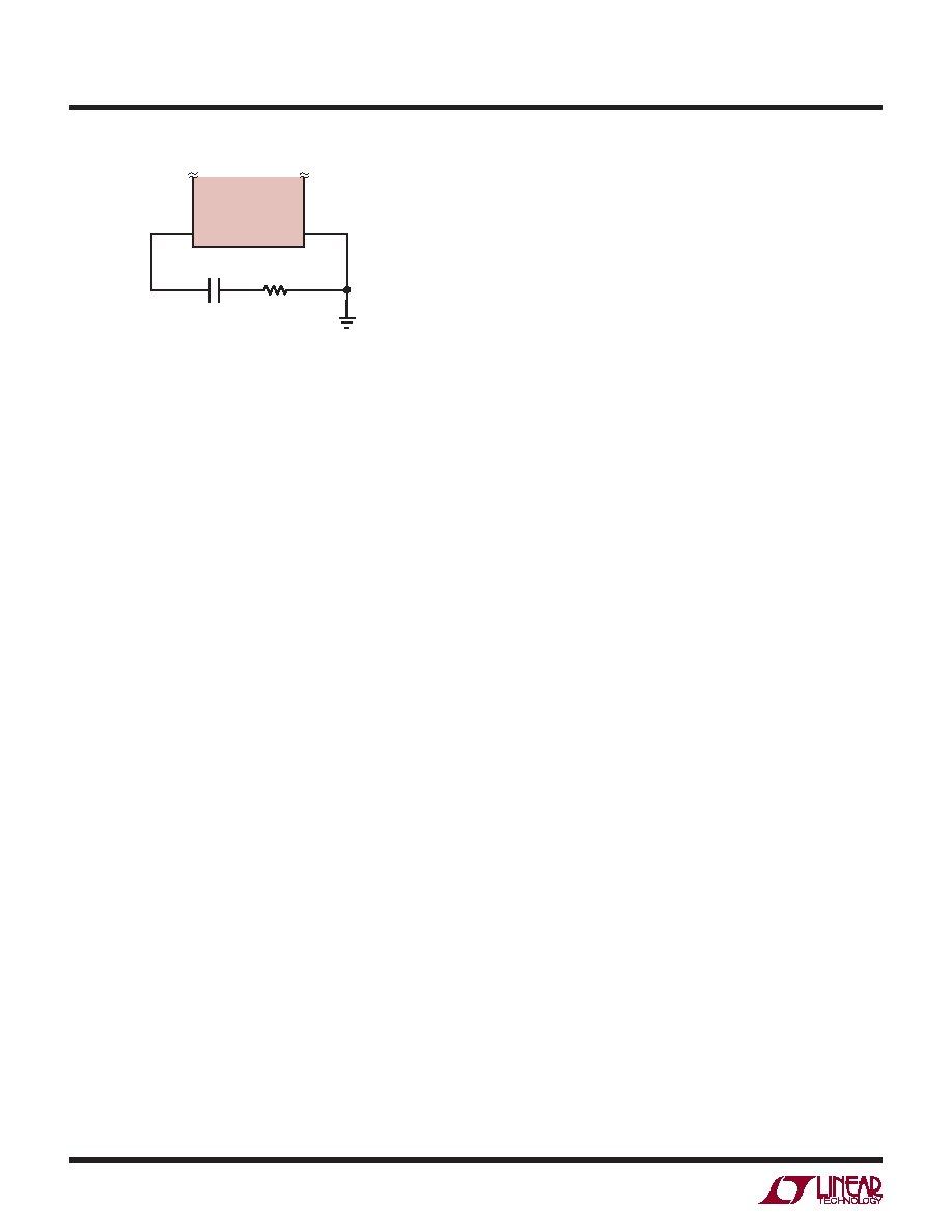
Figure 15. Main Loop Compensation for a Nonisolated Design
LTC4267
CC
RZ
ITH/RUN
PGND
4267 F15
相关PDF资料 |
PDF描述 |
|---|---|
| P1812R-104K | INDUCTOR POWER 100UH SMD |
| EBA28DTKN-S288 | CONN EDGECARD 56POS .125 EXTEND |
| A3AAB-2606M | IDC CABLE- ASC26B/AE26M/ASC26B |
| EB41-S0K1060X | CONN EDGEBOARD DUAL 20POS 3A |
| H3AKH-3018G | IDC CABLE - HSC30H/AE30G/HPK30H |
相关代理商/技术参数 |
参数描述 |
|---|---|
| DC-85FMMT | 制造商:Polycase 功能描述:Enclosure;Flanged;PanelMount;ABS,UL94-5VA;Black;8.25x5x4.33 In;DC Series |
| DC-85FMMT01 | 制造商:Polycase 功能描述:Enclosure;Flanged;PanelMount;ABS,UL94-5VA;Gray;8.25x5x4.33 In;DC Series |
| DC-85PMMT | 制造商:Polycase 功能描述:Enclosure;Box-Lid;Desktop;ABS,UL94-5VA;Black;8.25x5x4.33 In;DC Series |
| DC-85PMMT01 | 制造商:Polycase 功能描述:Enclosure;Box-Lid;Desktop;ABS,UL94-5VA;Gray;8.25x5x4.33 In;DC Series |
| DC872A | 制造商:Linear Technology 功能描述:DEMO BOARD FOR LTC4213CDD 制造商:Linear Technology 功能描述:EVAL BOARD, LTC4213CDD OVERVOLTAGE PROT |
发布紧急采购,3分钟左右您将得到回复。