- 您现在的位置:买卖IC网 > PDF目录16615 > DC859A (Linear Technology)EVAL BOARD FOR LTC4267 PDF资料下载
参数资料
| 型号: | DC859A |
| 厂商: | Linear Technology |
| 文件页数: | 27/32页 |
| 文件大小: | 0K |
| 描述: | EVAL BOARD FOR LTC4267 |
| 设计资源: | DC859A Design File DC859A Schematic |
| 标准包装: | 1 |
| 主要目的: | 电源管理,以太网供电(POE) |
| 嵌入式: | 否 |
| 已用 IC / 零件: | LTC4267 |
| 已供物品: | 板 |
第1页第2页第3页第4页第5页第6页第7页第8页第9页第10页第11页第12页第13页第14页第15页第16页第17页第18页第19页第20页第21页第22页第23页第24页第25页第26页当前第27页第28页第29页第30页第31页第32页
LTC4267
4
4267fc
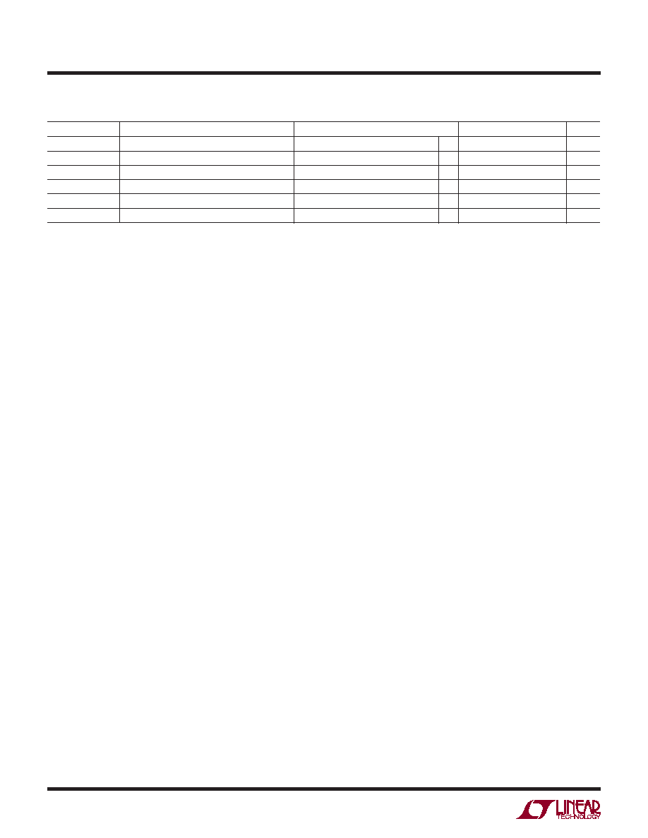
The ● denotes the specications which apply over the full operating
temperature range, otherwise specications are at TA = 25°C. (Note 3)
SYMBOL
PARAMETER
CONDITIONS
MIN
TYP
MAX
UNITS
tRISE
NGATE Drive Rise Time
CLOAD = 3000pF, PVCC – PGND = 8V
40
ns
tFALL
NGATE Drive Fall Time
CLOAD = 3000pF, PVCC – PGND = 8V
40
ns
VIMAX
Peak Current Sense Voltage
RSL = 0, PVCC – PGND = 8V (Note 16)
●
90
100
115
mV
ISLMAX
Peak Slope Compensation Output Current
PVCC – PGND = 8V (Note 17)
5
A
tSFST
Soft-Start Time
PVCC – PGND = 8V
1.4
ms
TSHUTDOWN
Thermal Shutdown Trip Temperature
(Notes 14, 18)
140
°C
Note 1: Stresses beyond those listed under Absolute Maximum Ratings
may cause permanent damage to the device. Exposure to any Absolute
Maximum Rating condition for extended periods may affect device
reliability and lifetime.
Note 2: PVCC internal clamp circuit self regulates to 9.4V with respect to
PGND.
Note 3: The LTC4267 operates with a negative supply voltage in the range
of – 1.5V to – 57V. To avoid confusion, voltages for the PD interface
are always referred to in terms of absolute magnitude. Terms such as
“maximum negative voltage” refer to the largest negative voltage and
a “rising negative voltage” refers to a voltage that is becoming more
negative.
Note 4: The LTC4267 is designed to work with two polarity protection
diode drops between the PSE and PD. Parameter ranges specied in the
Electrical Characteristics section are with respect to this product pins and
are designed to meet IEEE 802.3af specications when these diode drops
are included. See the Application Information section.
Note 5: Signature resistance is measured via the two-point ΔV/ΔI method
as dened by IEEE 802.3af. The PD signature resistance is offset from the
25kΩ to account for diode resistance. With two series diodes, the total PD
resistance will be between 23.75kΩ and 26.25kΩ and meet IEEE 802.3af
specications. The minimum probe voltages measured at the LTC4267
pins are – 1.5V and – 2.5V. The maximum probe voltages are – 8.5V and
– 9.5V.
Note 6: The PD interface includes hysteresis in the UVLO voltages to
preclude any start-up oscillation. Per IEEE 802.3af requirements, the PD
will power up from a voltage source with 20Ω series resistance on the rst
trial.
Note 7: Dynamic Supply current is higher due to the gate charge being
delivered at the switching frequency.
Note 8: IVPORTN_CLASS does not include classication current
programmed at the RCLASS pin. Total current in classication mode will be
IVPORTN_CLASS + ICLASS (See note 9).
Note 9: ICLASS is the measured current owing through RCLASS. ΔICLASS
accuracy is with respect to the ideal current dened as ICLASS = 1.237/
RCLASS. The current accuracy does not include variations in RCLASS
resistance. The total classication current for a PD also includes the IC
quiescent current (IVPORTN_CLASS). See Applications Information.
Note 10: For the DHC package, this parameter is assured by design and
wafer level testing.
Note 11: To disable the 25kΩ signature, tie SIGDISA to VPORTP or hold
SIGDISA high with respect to VPORTN. See Applications Information.
Note 12: The switching regulator is tested in a feedback loop that servos
VFB to the output of the error amplier while maintaining ITH/RUN at the
midpoint of the current limit range.
Note 13: IPOUT_LEAK includes current drawn through POUT by the power
good status circuit. This current is compensated for in the 25kΩ signature
resistance and does not affect PD operation.
Note 14: The LTC4267 PD Interface includes thermal protection. In the
event of an overtemperature condition, the PD interface will turn off
the switching regulator until the part cools below the overtemperature
limit. The LTC4267 is also protected against thermal damage from
incorrect classication probing by the PSE. If the LTC4267 exceeds the
overtemperature threshold, the classication load current is disabled.
Note 15: The PD interface includes dual level input current limit. At turn-
on, before the POUT load capacitor is charged, the PD current level is set
to a low level. After the load capacitor is charged and the POUT – VPORTN
voltage difference is below the power good threshold, the PD switches to
high level current limit. The PD stays in high level current limit until the
input voltage drops below the UVLO turn-off threshold.
Note 16: Peak current sense voltage is reduced dependent on duty cycle
and an optional external resistor in series with the SENSE pin (RSL). For
details, refer to the programmable slope compensation feature in the
Applications Information section.
Note 17: Guaranteed by design.
Note 18: The PD interface includes overtemperature protection that is
intended to protect the device from momentary overload conditions.
Junction temperature will exceed 125°C when overtemperature protection
is active. Continuous operation above the specied maximum operating
junction temperature may impair device reliability.
ELECTRICAL CHARACTERISTICS
相关PDF资料 |
PDF描述 |
|---|---|
| P1812R-104K | INDUCTOR POWER 100UH SMD |
| EBA28DTKN-S288 | CONN EDGECARD 56POS .125 EXTEND |
| A3AAB-2606M | IDC CABLE- ASC26B/AE26M/ASC26B |
| EB41-S0K1060X | CONN EDGEBOARD DUAL 20POS 3A |
| H3AKH-3018G | IDC CABLE - HSC30H/AE30G/HPK30H |
相关代理商/技术参数 |
参数描述 |
|---|---|
| DC-85FMMT | 制造商:Polycase 功能描述:Enclosure;Flanged;PanelMount;ABS,UL94-5VA;Black;8.25x5x4.33 In;DC Series |
| DC-85FMMT01 | 制造商:Polycase 功能描述:Enclosure;Flanged;PanelMount;ABS,UL94-5VA;Gray;8.25x5x4.33 In;DC Series |
| DC-85PMMT | 制造商:Polycase 功能描述:Enclosure;Box-Lid;Desktop;ABS,UL94-5VA;Black;8.25x5x4.33 In;DC Series |
| DC-85PMMT01 | 制造商:Polycase 功能描述:Enclosure;Box-Lid;Desktop;ABS,UL94-5VA;Gray;8.25x5x4.33 In;DC Series |
| DC872A | 制造商:Linear Technology 功能描述:DEMO BOARD FOR LTC4213CDD 制造商:Linear Technology 功能描述:EVAL BOARD, LTC4213CDD OVERVOLTAGE PROT |
发布紧急采购,3分钟左右您将得到回复。