参数资料
| 型号: | DS3120N |
| 厂商: | Maxim Integrated Products |
| 文件页数: | 61/133页 |
| 文件大小: | 0K |
| 描述: | IC FRAMER T1 28-CHANNEL IND |
| 标准包装: | 1 |
| 控制器类型: | T1 调帧器 |
| 接口: | 并行/串行 |
| 电源电压: | 2.97 V ~ 3.63 V |
| 电流 - 电源: | 300mA |
| 工作温度: | -40°C ~ 85°C |
| 安装类型: | 表面贴装 |
| 封装/外壳: | 316-BGA |
| 包装: | 管件 |
第1页第2页第3页第4页第5页第6页第7页第8页第9页第10页第11页第12页第13页第14页第15页第16页第17页第18页第19页第20页第21页第22页第23页第24页第25页第26页第27页第28页第29页第30页第31页第32页第33页第34页第35页第36页第37页第38页第39页第40页第41页第42页第43页第44页第45页第46页第47页第48页第49页第50页第51页第52页第53页第54页第55页第56页第57页第58页第59页第60页当前第61页第62页第63页第64页第65页第66页第67页第68页第69页第70页第71页第72页第73页第74页第75页第76页第77页第78页第79页第80页第81页第82页第83页第84页第85页第86页第87页第88页第89页第90页第91页第92页第93页第94页第95页第96页第97页第98页第99页第100页第101页第102页第103页第104页第105页第106页第107页第108页第109页第110页第111页第112页第113页第114页第115页第116页第117页第118页第119页第120页第121页第122页第123页第124页第125页第126页第127页第128页第129页第130页第131页第132页第133页
DS3112
33 of 133
4
MASTER DEVICE CONFIGURATION AND STATUS/INTERRUPT
4.1 Master Reset and ID Register Description
The master reset and ID (MRID) register can be used to globally reset the device. When the
RST bit is set
to one, all of the internal registers will be placed into their default state, which is 0000h. A reset can also
be invoked by the
RST hardware signal.
The upper byte of the MRID register is read-only and it can be read by the host to determine the chip
revision. Contact the factory for specifics on the meaning of the value read from the ID0 to ID7 bits.
Register Name:
MRID
Register Description:
Master Reset and ID Register
Register Address:
00h
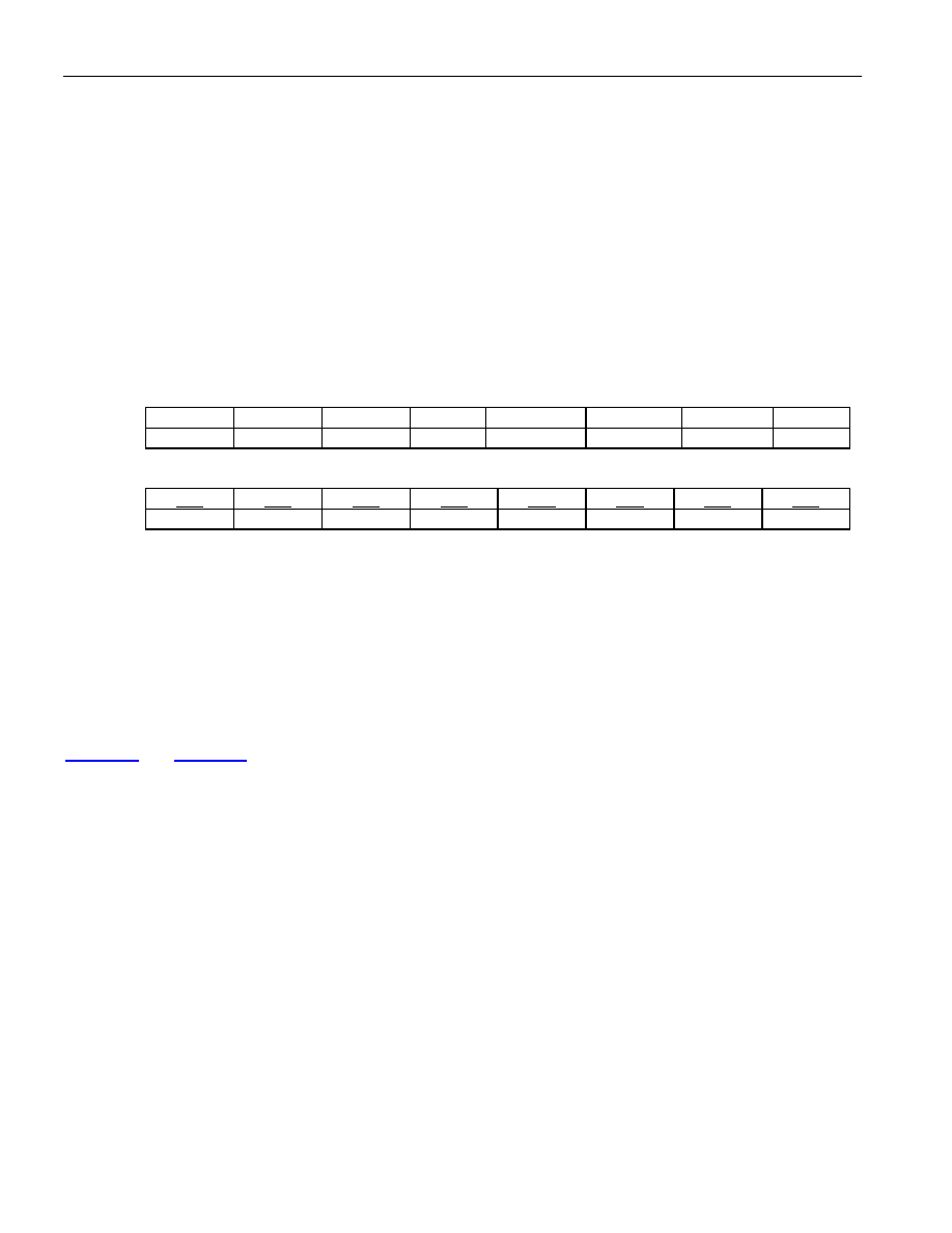
Bit #
7
6
5
4
3
2
1
0
Name
—
T3E3RSY
T2E2RSY
RFIFOR
RST
Default
—
0
Bit #
15
14
13
12
11
10
9
8
Name
ID7
ID6
ID5
ID4
ID3
ID2
ID1
ID0
Default
X
Note: Bits that are underlined are read-only; all other bits are read-write.
Bit 0: Master Software Reset (RST). When this bit is set to a one by the host, it will force all of the internal
registers to their default state, which is 0000h and forces the T3/E3 and T1/E1 outputs to send an all ones pattern.
This bit must be set high for a minimum of 100ns. This software bit is logically ORed with the hardware signal
RST.
0 = normal operation
1 = force all internal registers to their default value of 0000h
Bit 1: Low-Speed (T1/E1) Receive FIFO Reset (RFIFOR). A zero to one transition on this bit will cause the
receive T1/E1 demux FIFOs to be reset, which will cause them to be flushed. See the DS3112 Block Diagrams in
Figure 1-1 and Figure 1-2 for details on the placement of the FIFOs within the chip. This bit must be cleared and
set again for a subsequent reset to occur.
Bit 2: T2/E2/G.747 Force Receive Framer Resynchronization (T2E2RSY). A zero to one transition on this bit
will cause all seven of the T2 receive framers or all four of the E2 receive framers or all seven of the G.747 framers
to resynchronize. This bit must be cleared and set again for a subsequent resynchronization to occur.
Bit 3: T3/E3 Force Receive Framer Resynchronization (T3E3RSY). A zero to one transition on this bit will
cause the T3 receive framer or the E3 receive framer to resynchronize. This bit must be cleared and set again for a
subsequent resynchronization to occur.
Bits 8 to 15: Chip Revision ID Bit 0 to 7 (ID0 to ID7). Read-only. Contact the factory for details on the meaning
of the ID bits.
相关PDF资料 |
PDF描述 |
|---|---|
| DS31256+ | IC CTRLR HDLC 256-CHANNEL 256BGA |
| DS3141+ | IC FRAMER DS3/E3 SNGL 144CSBGA |
| DS31412N | IC 12CH DS3/3 FRAMER 349-BGA |
| DS3150TN | IC LIU T3/E3/STS-1 IND 48-TQFP |
| DS3154N+ | IC LIU DS3/E3/STS-1 QD 144CSBGA |
相关代理商/技术参数 |
参数描述 |
|---|---|
| DS3121 | 功能描述:IC TGATOR T1-T3 AGGREGATOR RoHS:否 类别:集成电路 (IC) >> 接口 - 控制器 系列:- 标准包装:4,900 系列:- 控制器类型:USB 2.0 控制器 接口:串行 电源电压:3 V ~ 3.6 V 电流 - 电源:135mA 工作温度:0°C ~ 70°C 安装类型:表面贴装 封装/外壳:36-VFQFN 裸露焊盘 供应商设备封装:36-QFN(6x6) 包装:* 其它名称:Q6396337A |
| DS3121N | 功能描述:IC TGATOR T1-T3 AGGREGATOR IND RoHS:否 类别:集成电路 (IC) >> 接口 - 控制器 系列:- 标准包装:4,900 系列:- 控制器类型:USB 2.0 控制器 接口:串行 电源电压:3 V ~ 3.6 V 电流 - 电源:135mA 工作温度:0°C ~ 70°C 安装类型:表面贴装 封装/外壳:36-VFQFN 裸露焊盘 供应商设备封装:36-QFN(6x6) 包装:* 其它名称:Q6396337A |
| DS31256 | 功能描述:输入/输出控制器接口集成电路 256Ch High Thruput HDLC Cntlr RoHS:否 制造商:Silicon Labs 产品: 输入/输出端数量: 工作电源电压: 最大工作温度:+ 85 C 最小工作温度:- 40 C 安装风格:SMD/SMT 封装 / 箱体:QFN-64 封装:Tray |
| DS31256+ | 功能描述:输入/输出控制器接口集成电路 256Ch High Thruput HDLC Cntlr RoHS:否 制造商:Silicon Labs 产品: 输入/输出端数量: 工作电源电压: 最大工作温度:+ 85 C 最小工作温度:- 40 C 安装风格:SMD/SMT 封装 / 箱体:QFN-64 封装:Tray |
| DS31256B | 功能描述:输入/输出控制器接口集成电路 256Ch High Thruput HDLC Cntlr RoHS:否 制造商:Silicon Labs 产品: 输入/输出端数量: 工作电源电压: 最大工作温度:+ 85 C 最小工作温度:- 40 C 安装风格:SMD/SMT 封装 / 箱体:QFN-64 封装:Tray |
发布紧急采购,3分钟左右您将得到回复。