- 您现在的位置:买卖IC网 > PDF目录10993 > DS3170N+ (Maxim Integrated Products)IC TXRX DS3/E3 100-CSBGA PDF资料下载
参数资料
| 型号: | DS3170N+ |
| 厂商: | Maxim Integrated Products |
| 文件页数: | 193/230页 |
| 文件大小: | 0K |
| 描述: | IC TXRX DS3/E3 100-CSBGA |
| 产品培训模块: | Lead (SnPb) Finish for COTS Obsolescence Mitigation Program |
| 标准包装: | 640 |
| 功能: | 单芯片收发器 |
| 接口: | DS3,E3 |
| 电路数: | 1 |
| 电源电压: | 3.135 V ~ 3.465 V |
| 电流 - 电源: | 120mA |
| 工作温度: | -40°C ~ 85°C |
| 安装类型: | 表面贴装 |
| 封装/外壳: | 100-LBGA,CSBGA |
| 供应商设备封装: | 100-CSBGA(11x11) |
| 包装: | 托盘 |
| 包括: | DS3 调帧器,E3 调帧器,HDLC 控制器,芯片内 BERT |
第1页第2页第3页第4页第5页第6页第7页第8页第9页第10页第11页第12页第13页第14页第15页第16页第17页第18页第19页第20页第21页第22页第23页第24页第25页第26页第27页第28页第29页第30页第31页第32页第33页第34页第35页第36页第37页第38页第39页第40页第41页第42页第43页第44页第45页第46页第47页第48页第49页第50页第51页第52页第53页第54页第55页第56页第57页第58页第59页第60页第61页第62页第63页第64页第65页第66页第67页第68页第69页第70页第71页第72页第73页第74页第75页第76页第77页第78页第79页第80页第81页第82页第83页第84页第85页第86页第87页第88页第89页第90页第91页第92页第93页第94页第95页第96页第97页第98页第99页第100页第101页第102页第103页第104页第105页第106页第107页第108页第109页第110页第111页第112页第113页第114页第115页第116页第117页第118页第119页第120页第121页第122页第123页第124页第125页第126页第127页第128页第129页第130页第131页第132页第133页第134页第135页第136页第137页第138页第139页第140页第141页第142页第143页第144页第145页第146页第147页第148页第149页第150页第151页第152页第153页第154页第155页第156页第157页第158页第159页第160页第161页第162页第163页第164页第165页第166页第167页第168页第169页第170页第171页第172页第173页第174页第175页第176页第177页第178页第179页第180页第181页第182页第183页第184页第185页第186页第187页第188页第189页第190页第191页第192页当前第193页第194页第195页第196页第197页第198页第199页第200页第201页第202页第203页第204页第205页第206页第207页第208页第209页第210页第211页第212页第213页第214页第215页第216页第217页第218页第219页第220页第221页第222页第223页第224页第225页第226页第227页第228页第229页第230页
DS3170 DS3/E3 Single-Chip Transceiver
65 of 230
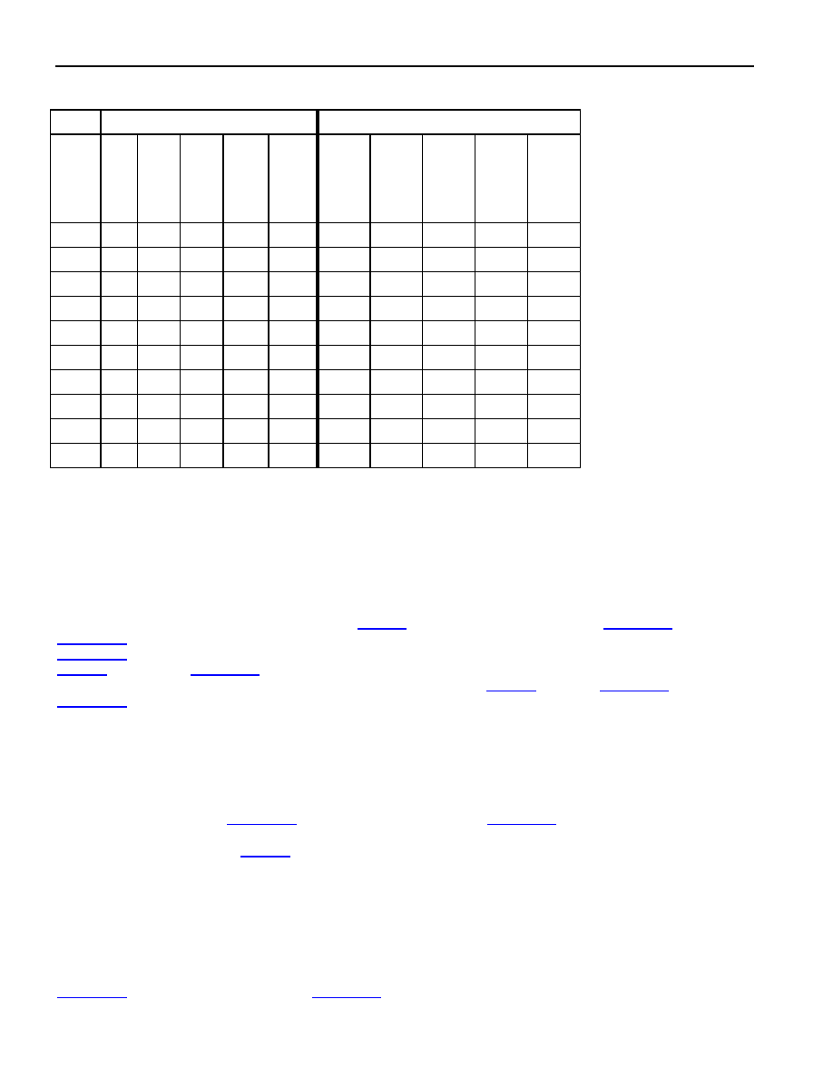
Table 10-10. Reset and Power-Down Sources
PIN
REGISTER BITS
INTERNAL SIGNALS
RS
T
G
:R
ST
G
:RS
T
DP
P:R
ST
P:R
ST
D
P
P:PD
Gl
oba
l
reset
Gl
oba
ld
p
reset
P
o
rt
reset
Po
rt
d
p
reset
P
o
rt
p
o
w
er
dn
0
F0
F1
F0
F1
1
F1
F0
F1
1
0
1
F1
0
1
0
1
0
X
1
0
1
0
1
0
1
0
X
0
1
0
1
0
1
0
1
F1
0
1
0
1
0
1
0
1
0
1
0
1
0
1
0
1
0
Register Bit States—F0: Forced to 0; F1: Forced to 1; 0: Set to 0; 1: Set to 1; X: Don’t care
Forced: Internally controlled; Set: User controlled
The reset signals in the device are asynchronous so they no not require a clock to put the logic into the reset state.
Clock signals may be needed to make the logic come out of the reset state.
The power-down function disables the appropriate clocks to cause the logic to generate a minimum of power. It
also puts the LIU circuits into the power-down mode. The 8KREF and ONESEC circuits can be powered down by
disabling the 8KREF source. The CLAD can also be powered down by disabling it.
After a global reset, all of the control and status registers are set to their default values and all the other flops are
reset to their reset values. The global register GL.CR1.RSTDP, and the port register PORT.CR1.RSTDP and
PORT.CR1.PD bits, are set after the global reset. A valid initialization sequence would be to clear the
PORT.CR1.PD bit, write to all of the configuration registers to set them in the desired modes, then clear the
GL.CR1.RSTDP and PORT.CR1.RSTDP bits. This would cause the logic in the port to start up in a repeatable
PORT.CR1.PD them writing to all of the configuration registers to set them in the desired modes, and clearing all of
the latched status bits. The second initialization scheme could cause the device to temporarily go into modes of
operation that were not requested, but will quickly go into the requested modes of operation.
Some of the IO pins are put in a known state at reset. The transmit LIU outputs TXP and TXN are quiet and will not
drive positive or negative pulses. The global IO pins (GPIO[7:0]) are set as inputs at global reset. The port output
pins (TLCLK, TPOS/TDAT, TNEG, TOHCLK, TOHSOF, TSOFO/TDEN, TCLKO/TGCLK, ROH, ROHCLK,
ROHSOF, RSER, RSOFO/RDEN, RCLKO/RGCLK) are driven low at global or port reset and should stay low until
The
processor port three-state output pins (D[15:0],
RDY, INT) are forced into the high impedance state when the RST
pin is active, but not when the GL.CR1.RST bit is active.
After reset, the device will be in the default configuration:: The latched status bits are enabled to be cleared on
write. The CLAD is disabled. The global 8KREF and one-second timers are disabled. The line interface is in B3ZS
mode and the LIU is disabled and the transmit line pins are also disabled. The frame mode is DS3 C-bit with
automatic downstream AIS on LOS or OOF is enabled and automatic RDI on LOF, LOS, SEF or AIS is enabled
and automatic FEBE is enabled. Transmit clock comes from the REFCLK pin. The pin inversion on all pins is
disabled.
Individual blocks are reset and powered down when not used determined by the settings in the line mode bits
PORT.CR2.LM[2:0] and framer mode bits PORT.CR2.FM[2:0].
相关PDF资料 |
PDF描述 |
|---|---|
| DS2151QB | IC TXRX T1 1-CHIP 5V LP 44-PLCC |
| DS21Q58LN+ | IC TXRX E1 QUAD 3.3V 100LQFP |
| DS26504LN+ | IC T1/E1/J1 64KCC ELEMENT 64LQFP |
| DS21352G | IC TXRX T1 1-CHIP 3.3V 100-BGA |
| DS2174QN+T&R | IC BERT ENHANCED 44-PLCC |
相关代理商/技术参数 |
参数描述 |
|---|---|
| DS3170N+ | 功能描述:网络控制器与处理器 IC DS3/E3 Single-Chip Transceiver RoHS:否 制造商:Micrel 产品:Controller Area Network (CAN) 收发器数量: 数据速率: 电源电流(最大值):595 mA 最大工作温度:+ 85 C 安装风格:SMD/SMT 封装 / 箱体:PBGA-400 封装:Tray |
| DS3170N+T&R | 制造商:Maxim Integrated Products 功能描述:SINGLE PORT DS3/E3 SCT T&R IND LF - Tape and Reel 制造商:Maxim Integrated Products 功能描述:IC TXRX DS3/E3 100CSBGA |
| DS3170N+T&R | 功能描述:网络控制器与处理器 IC DS3/E3 Single-Chip Transceiver RoHS:否 制造商:Micrel 产品:Controller Area Network (CAN) 收发器数量: 数据速率: 电源电流(最大值):595 mA 最大工作温度:+ 85 C 安装风格:SMD/SMT 封装 / 箱体:PBGA-400 封装:Tray |
| DS3171 | 功能描述:网络控制器与处理器 IC Single DS3/E3 Single Chip Transceiver RoHS:否 制造商:Micrel 产品:Controller Area Network (CAN) 收发器数量: 数据速率: 电源电流(最大值):595 mA 最大工作温度:+ 85 C 安装风格:SMD/SMT 封装 / 箱体:PBGA-400 封装:Tray |
| DS3171N | 功能描述:网络控制器与处理器 IC Single DS3/E3 Single Chip Transceiver RoHS:否 制造商:Micrel 产品:Controller Area Network (CAN) 收发器数量: 数据速率: 电源电流(最大值):595 mA 最大工作温度:+ 85 C 安装风格:SMD/SMT 封装 / 箱体:PBGA-400 封装:Tray |
发布紧急采购,3分钟左右您将得到回复。