- 您现在的位置:买卖IC网 > PDF目录16559 > EV-ADF4153SD1Z (Analog Devices Inc)BOARD EVAL FOR ADF4153SD1Z PDF资料下载
参数资料
| 型号: | EV-ADF4153SD1Z |
| 厂商: | Analog Devices Inc |
| 文件页数: | 13/24页 |
| 文件大小: | 0K |
| 描述: | BOARD EVAL FOR ADF4153SD1Z |
| 标准包装: | 1 |
| 系列: | * |
ADF4153
Data Sheet
Rev. F | Page 20 of 24
Reference Spurs
Reference spurs are generally not a problem in fractional-N
synthesizers because the reference offset is far outside the
loop bandwidth. However, any reference feedthrough mechan-
ism that bypasses the loop can cause a problem. One such
mechanism is feedthrough of low levels of on-chip reference
switching noise out through the RFIN pin back to the VCO,
resulting in reference spur levels as high as –90 dBc. Care
should be taken in the PCB layout to ensure that the VCO
is well separated from the input reference to avoid a possible
feed-through path on the board.
SPUR CONSISTENCY
When jumping from Frequency A to Frequency B and then
back again using some fractional-N synthesizers, the spur levels
often differ each time Frequency A is programmed. However,
in the ADF4153, the spur levels on any particular channel are
always consistent.
PHASE RESYNC
The output of a fractional-N PLL can settle to any one of MOD
phase offsets with respect to the input reference, where MOD
is the fractional modulus. The phase resync feature in the
ADF4153 can be used to produce a consistent output phase
offset with respect to the input reference. This is necessary
in applications where the output phase and frequency are
important, such as digital beam-forming.
When phase resync is enabled, an internal timer generates sync
signals at intervals of tSYNC given by the following formula:
tSYNC = RESYNC × RESYNC_DELAY × tPFD
where tPFD is the PFD reference period.
RESYNC is the decimal value programmed in Bits DB[15…12]
of Register R2 and can be any integer in the range of 1 to 15. If
RESYNC is programmed to its default value of all zeros, then
the phase resync feature is disabled.
If phase resync is enabled, then RESYNC_DELAY must be
programmed to a value that is an integer multiple of the value
of MOD. RESYNC_DELAY is the decimal value programmed
into the MOD bits (DB[13…3] of Register R1 when load
control (Bit DB23 of Register R1) = 1.
When a new frequency is programmed, the second next sync
pulse after the LE rising edge is used to resynchronize the output
phase to the reference. The tSYNC time should be programmed to
a value that is at least as long as the worst-case lock time. Doing
so guarantees that the phase resync occurs after the last cycle
slip in the PLL settling transient.
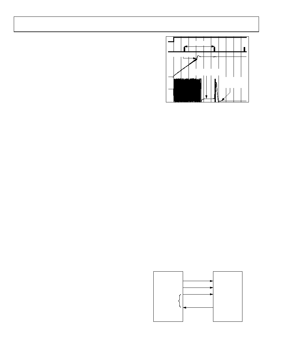
In the example shown in Figure 17, the PFD reference is
25 MHz and MOD = 125 for a 200 kHz channel spacing.
tSYNC is set to 400 s by programming RESYNC = 10 and
RESYNC_DELAY = 1000.
LE
PHASE
FREQUENCY
SYNC
(INTERNAL)
–100
0
100
200
1000
300
400
500
600
700
800
900
03685-
030
TIME (s)
PLL SETTLES TO
CORRECT PHASE
AFTER RESYNC
LAST CYCLE SLIP
PLL SETTLES TO
INCORRECT PHASE
tSYNC
Figure 17. Phase Resync Example
FILTER DESIGN—ADIsimPLL
A filter design and analysis program is available to help the user
implement PLL design. Visit www.analog.com/pll for a free
download of the ADIsimPLL software. The software designs,
simulates, and analyzes the entire PLL frequency domain and
time domain response. Various passive and active filter
architectures are allowed.
INTERFACING
The ADF4153 has a simple SPI-compatible serial interface
for writing to the device. CLK, DATA, and LE control the data
transfer. When latch enable (LE) is high, the 22 bits that are
clocked into the input register on each rising edge of SCLK are
transferred to the appropriate latch. See Figure 2 for the timing
diagram and Table 5 for the register truth table.
The maximum allowable serial clock rate is 20 MHz.
ADuC812 Interface
Figure 18 shows the interface between the ADF4153 and the
ADuC812 MicroConverter. Because the ADuC812 is based on
an 8051 core, this interface can be used with any 8051-based
micro-controller. The MicroConverter is set up for SPI master
mode with CPHA = 0. To initiate the operation, the I/O port
driving LE is brought low. Each latch of the ADF4153 needs a 24-
bit word, which is accomplished by writing three 8-bit bytes from
the MicroConverter to the device. After the third byte is written,
the LE input should be brought high to complete the transfer.
ADuC812
ADF4153
SCLOCK
CLK
DATA
LE
MUXOUT
(LOCK DETECT)
MOSI
I/O PORTS
03685-
024
Figure 18. ADuC812 to ADF4153 Interface
相关PDF资料 |
PDF描述 |
|---|---|
| MAX5059EUI+T | IC DRVR SYNC RECT 28-TSSOP |
| TCM809TVNB713 | IC RESET MONITOR 3.08V SOT23B-3 |
| GMM10DREI | CONN EDGECARD 20POS .156 EYELET |
| A1DXB-2036M | IDC CABLE- AKR20B/AE20M/X |
| H1WXH-1436M | IDC CABLE - HPL14H/AE14M/X |
相关代理商/技术参数 |
参数描述 |
|---|---|
| EV-ADF4156SD1Z | 功能描述:BOARD EVAL FOR ADF4156 RoHS:是 类别:编程器,开发系统 >> 评估演示板和套件 系列:- 标准包装:1 系列:- 主要目的:电信,线路接口单元(LIU) 嵌入式:- 已用 IC / 零件:IDT82V2081 主要属性:T1/J1/E1 LIU 次要属性:- 已供物品:板,电源,线缆,CD 其它名称:82EBV2081 |
| EV-ADF4157SD1Z | 功能描述:BOARD EVAL FOR ADF4157 RoHS:是 类别:编程器,开发系统 >> 评估演示板和套件 系列:- 标准包装:1 系列:- 主要目的:电信,线路接口单元(LIU) 嵌入式:- 已用 IC / 零件:IDT82V2081 主要属性:T1/J1/E1 LIU 次要属性:- 已供物品:板,电源,线缆,CD 其它名称:82EBV2081 |
| EV-ADF4159EB1Z | 制造商:Analog Devices 功能描述:EVALUATION BOARD - Boxed Product (Development Kits) 制造商:Analog Devices 功能描述:EVAL BOARD FOR ADF4159 |
| EV-ADF4159EB2Z | 制造商:Analog Devices 功能描述:13GHZFRAC-NPLL+ADF55XXVCO+3VADM - Boxed Product (Development Kits) |
| EV-ADF4159EB3Z | 制造商:Analog Devices 功能描述:EVALUATIONBOARD - Boxed Product (Development Kits) 制造商:Analog Devices 功能描述:EVAL BOARD FOR ADF4159 制造商:Analog Devices 功能描述:Clock & Timer Development Tools ADF4159 EVAL BRD |
发布紧急采购,3分钟左右您将得到回复。