- 您现在的位置:买卖IC网 > PDF目录16559 > EV-ADF4153SD1Z (Analog Devices Inc)BOARD EVAL FOR ADF4153SD1Z PDF资料下载
参数资料
| 型号: | EV-ADF4153SD1Z |
| 厂商: | Analog Devices Inc |
| 文件页数: | 14/24页 |
| 文件大小: | 0K |
| 描述: | BOARD EVAL FOR ADF4153SD1Z |
| 标准包装: | 1 |
| 系列: | * |
Data Sheet
ADF4153
Rev. F | Page 21 of 24
When operating in this mode, the maximum SCLOCK rate of
the ADuC812 is 4 MHz. This means that the maximum rate at
which the output frequency can be changed is 180 kHz.
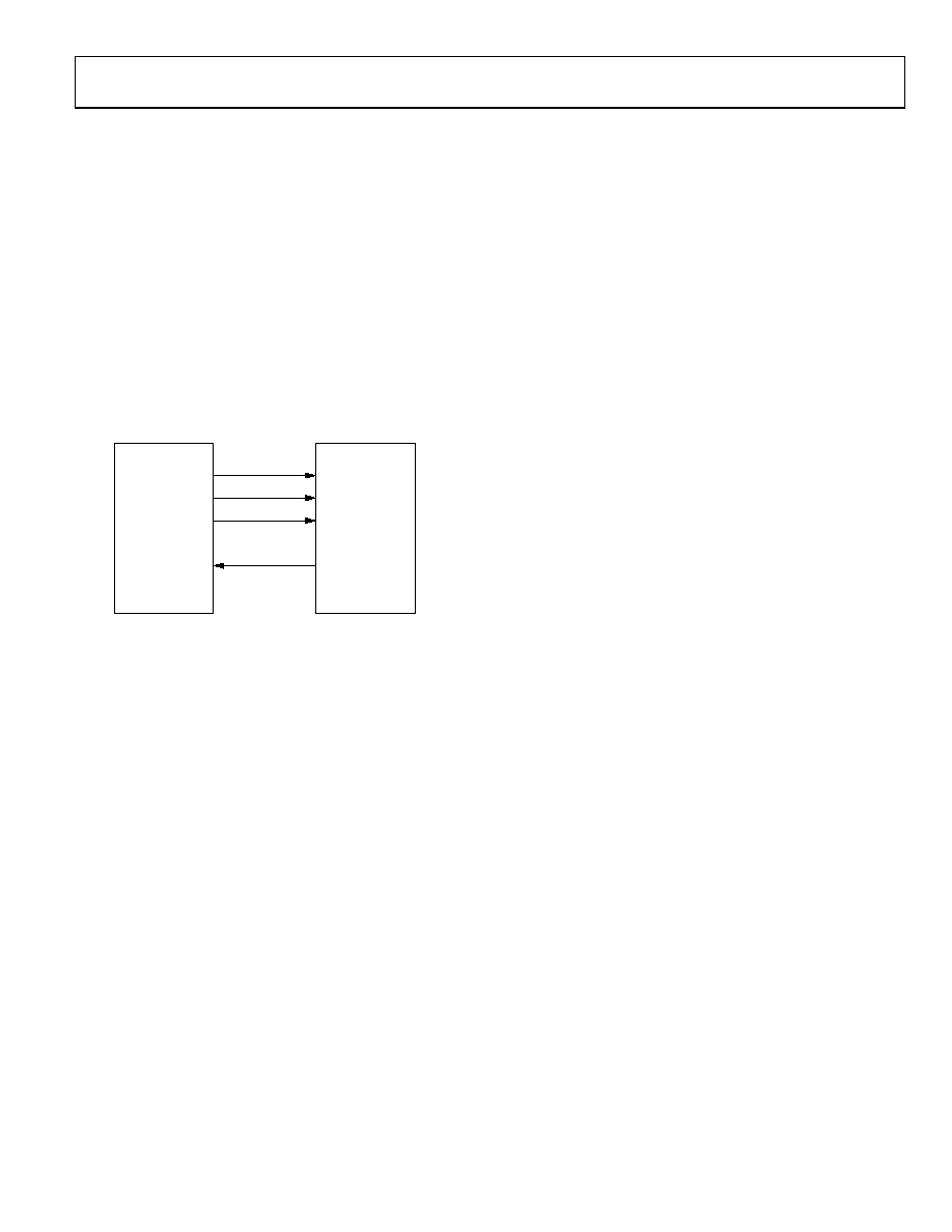
ADSP-21xx Interface
Figure 19 shows the interface between the ADF4153 and the
ADSP-21xx digital signal processor. As discussed previously,
the ADF4153 needs a 24-bit serial word for each latch write.
The easiest way to accomplish this using the ADSP-21xx family
is to use the autobuffered transmit mode of operation with
alternate framing. This provides a means for transmitting an
entire block of serial data before an interrupt is generated.
Set up the word length for eight bits and use three memory
locations for each 24-bit word. To program each 24-bit latch,
store the three 8-bit bytes, enable the autobuffered mode, and
write to the transmit register of the DSP. This last operation
initiates the autobuffer transfer.
ADSP-21xx
ADF4153
SCLK
CLK
DATA
LE
MUXOUT
(LOCK DETECT)
DT
TFS
I/O FLAGS
03685-
025
Figure 19. ADSP-21xx to ADF4153 Interface
PCB DESIGN GUIDELINES FOR CHIP SCALE
PACKAGE
The lands on the chip scale package (CP-20) are rectangular.
The printed circuit board (PCB) pad for these should be 0.1 mm
longer than the package land length and 0.05 mm wider than
the package land width. The land should be centered on the
pad. This ensures that the solder joint size is maximized.
The bottom of the chip scale package has a central thermal pad.
The thermal pad on the PCB should be at least as large as this
exposed pad. On the PCB, there should be a clearance of at least
0.25 mm between the thermal pad and the inner edges of the
pad pattern. This ensures that shorting is avoided.
Thermal vias can be used on the PCB thermal pad to improve
thermal performance of the package. If vias are used, they should
be incorporated in the thermal pad at 1.2 mm pitch grid. The
via diameter should be between 0.3 mm and 0.33 mm, and the
via barrel should be plated with one ounce of copper to plug the
via. The user should connect the PDB thermal pad to AGND.
相关PDF资料 |
PDF描述 |
|---|---|
| MAX5059EUI+T | IC DRVR SYNC RECT 28-TSSOP |
| TCM809TVNB713 | IC RESET MONITOR 3.08V SOT23B-3 |
| GMM10DREI | CONN EDGECARD 20POS .156 EYELET |
| A1DXB-2036M | IDC CABLE- AKR20B/AE20M/X |
| H1WXH-1436M | IDC CABLE - HPL14H/AE14M/X |
相关代理商/技术参数 |
参数描述 |
|---|---|
| EV-ADF4156SD1Z | 功能描述:BOARD EVAL FOR ADF4156 RoHS:是 类别:编程器,开发系统 >> 评估演示板和套件 系列:- 标准包装:1 系列:- 主要目的:电信,线路接口单元(LIU) 嵌入式:- 已用 IC / 零件:IDT82V2081 主要属性:T1/J1/E1 LIU 次要属性:- 已供物品:板,电源,线缆,CD 其它名称:82EBV2081 |
| EV-ADF4157SD1Z | 功能描述:BOARD EVAL FOR ADF4157 RoHS:是 类别:编程器,开发系统 >> 评估演示板和套件 系列:- 标准包装:1 系列:- 主要目的:电信,线路接口单元(LIU) 嵌入式:- 已用 IC / 零件:IDT82V2081 主要属性:T1/J1/E1 LIU 次要属性:- 已供物品:板,电源,线缆,CD 其它名称:82EBV2081 |
| EV-ADF4159EB1Z | 制造商:Analog Devices 功能描述:EVALUATION BOARD - Boxed Product (Development Kits) 制造商:Analog Devices 功能描述:EVAL BOARD FOR ADF4159 |
| EV-ADF4159EB2Z | 制造商:Analog Devices 功能描述:13GHZFRAC-NPLL+ADF55XXVCO+3VADM - Boxed Product (Development Kits) |
| EV-ADF4159EB3Z | 制造商:Analog Devices 功能描述:EVALUATIONBOARD - Boxed Product (Development Kits) 制造商:Analog Devices 功能描述:EVAL BOARD FOR ADF4159 制造商:Analog Devices 功能描述:Clock & Timer Development Tools ADF4159 EVAL BRD |
发布紧急采购,3分钟左右您将得到回复。