- 您现在的位置:买卖IC网 > PDF目录16871 > EVAL-AD5522EBDZ (Analog Devices Inc)BOARD EVAL FOR 14X14MM AD5522 PDF资料下载
参数资料
| 型号: | EVAL-AD5522EBDZ |
| 厂商: | Analog Devices Inc |
| 文件页数: | 3/64页 |
| 文件大小: | 0K |
| 描述: | BOARD EVAL FOR 14X14MM AD5522 |
| 标准包装: | 1 |
| 主要目的: | 测试与测量,参数测量单元(PMU) |
| 已用 IC / 零件: | AD5522 |
| 已供物品: | 板 |
第1页第2页当前第3页第4页第5页第6页第7页第8页第9页第10页第11页第12页第13页第14页第15页第16页第17页第18页第19页第20页第21页第22页第23页第24页第25页第26页第27页第28页第29页第30页第31页第32页第33页第34页第35页第36页第37页第38页第39页第40页第41页第42页第43页第44页第45页第46页第47页第48页第49页第50页第51页第52页第53页第54页第55页第56页第57页第58页第59页第60页第61页第62页第63页第64页
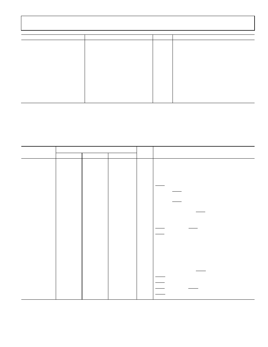
Data Sheet
AD5522
Rev. E | Page 11 of 64
Parameter
Min
Typ 1
Max
Unit
Test Conditions/Comments
Power Supply Sensitivity2
From dc to 1 kHz
ΔForced Voltage/ΔAVDD
80
dB
ΔForced Voltage/ΔAVSS
80
dB
ΔMeasured Current/ΔAVDD
85
dB
ΔMeasured Current/ΔAVSS
75
dB
ΔForced Current/ΔAVDD
75
dB
ΔForced Current/ΔAVSS
75
dB
ΔMeasured Voltage/ΔAVDD
85
dB
ΔMeasured Voltage/ΔAVSS
80
dB
ΔForced Voltage/ΔDVCC
90
dB
ΔMeasured Current/ΔDVCC
90
dB
ΔForced Current/ΔDVCC
90
dB
ΔMeasured Voltage/ΔDVCC
90
dB
1
Typical specifications are at 25°C and nominal supply, ±15.25 V, unless otherwise noted.
2
Guaranteed by design and characterization; not production tested. Tempco values are mean and standard deviation, unless otherwise noted.
TIMING CHARACTERISTICS
AVDD ≥ 10 V, AVSS ≤ 5 V, |AVDD AVSS| ≥ 20 V and ≤ 33 V, DVCC = 2.3 V to 5.25 V, VREF = 5 V, TJ = 25°C to 90°C, unless
otherwise noted.
Table 2. SPI Interface
DVCC, Limit at TMIN, TMAX
Unit
Description
2.3V to 2.7V
2.7V to 3.6V
4.5V to 5.25V
tWRITE4
1030
735
ns min
Single channel update cycle time (X1 register write)
950
655
ns min
Single channel update cycle time (any other register write)
t1
30
20
ns min
SCLK cycle time
t2
8
ns min
SCLK high time
t3
8
ns min
SCLK low time
t4
10
ns min
SYNC falling edge to SCLK falling edge setup time
150
ns min
Minimum SYNC high time in write mode after X1 register
write (one channel)
70
ns min
Minimum SYNC high time in write mode after any
other register write
t6
10
5
ns min
29th SCLK falling edge to SYNC rising edge
t7
5
ns min
Data setup time
t8
9
7
4.5
ns min
Data hold time
t9
120
75
55
ns max
SYNC rising edge to BUSY falling edge
t10
BUSY pulse width low for X1 and some PMU register writes;
1 DAC X1
1.65
s max
2 DAC X1
2.3
s max
3 DAC X1
2.95
s max
4 DAC X1
3.6
s max
Other Registers
270
ns max
System control register/PMU registers
t11
20
ns min
29th SCLK falling edge to LOAD falling edge
t12
20
ns min
LOAD pulse width low
t13
150
ns min
BUSY rising edge to FOHx output response time
t14
0
ns min
BUSY rising edge to LOAD falling edge
t15
100
ns max
LOAD falling edge to FOHx output response time
相关PDF资料 |
PDF描述 |
|---|---|
| EVAL-AD5520EBZ | BOARD EVAL FOR AD5520 |
| MAX6198AESA+T | IC VREF SERIES PREC 4.096V 8SOIC |
| QPI-5-EVAL1 | EVALUATION BOARD FOR QPI-5 |
| H6MMH-4006M | DIP CABLE - HDM40H/AE40M/HDM40H |
| QPO-2-EVAL1 | EVALUATION BOARD FOR QPO-2 |
相关代理商/技术参数 |
参数描述 |
|---|---|
| EVAL-AD5522EBUZ | 功能描述:BOARD EVAL FOR 12X12MM AD5522 RoHS:是 类别:编程器,开发系统 >> 评估演示板和套件 系列:- 标准包装:1 系列:- 主要目的:电信,线路接口单元(LIU) 嵌入式:- 已用 IC / 零件:IDT82V2081 主要属性:T1/J1/E1 LIU 次要属性:- 已供物品:板,电源,线缆,CD 其它名称:82EBV2081 |
| EVAL-AD5532EB | 制造商:AD 制造商全称:Analog Devices 功能描述:32-Channel Infinite Sample-and-Hold |
| EVAL-AD5532EBZ | 功能描述:BOARD EVAL FOR AD5532 RoHS:是 类别:编程器,开发系统 >> 评估板 - 数模转换器 (DAC) 系列:- 产品培训模块:Lead (SnPb) Finish for COTS Obsolescence Mitigation Program 标准包装:1 系列:- DAC 的数量:4 位数:12 采样率(每秒):- 数据接口:串行,SPI? 设置时间:3µs DAC 型:电流/电压 工作温度:-40°C ~ 85°C 已供物品:板 已用 IC / 零件:MAX5581 |
| EVAL-AD5532HSEBZ | 功能描述:BOARD EVAL FOR AD5532HS RoHS:是 类别:编程器,开发系统 >> 评估板 - 数模转换器 (DAC) 系列:- 产品培训模块:Lead (SnPb) Finish for COTS Obsolescence Mitigation Program 标准包装:1 系列:- DAC 的数量:4 位数:12 采样率(每秒):- 数据接口:串行,SPI? 设置时间:3µs DAC 型:电流/电压 工作温度:-40°C ~ 85°C 已供物品:板 已用 IC / 零件:MAX5581 |
| EVAL-AD5533EB | 制造商:AD 制造商全称:Analog Devices 功能描述:32-Channel Precision Infinite Sample-and-Hold |
发布紧急采购,3分钟左右您将得到回复。