- 您现在的位置:买卖IC网 > PDF目录16871 > EVAL-AD5522EBDZ (Analog Devices Inc)BOARD EVAL FOR 14X14MM AD5522 PDF资料下载
参数资料
| 型号: | EVAL-AD5522EBDZ |
| 厂商: | Analog Devices Inc |
| 文件页数: | 38/64页 |
| 文件大小: | 0K |
| 描述: | BOARD EVAL FOR 14X14MM AD5522 |
| 标准包装: | 1 |
| 主要目的: | 测试与测量,参数测量单元(PMU) |
| 已用 IC / 零件: | AD5522 |
| 已供物品: | 板 |
第1页第2页第3页第4页第5页第6页第7页第8页第9页第10页第11页第12页第13页第14页第15页第16页第17页第18页第19页第20页第21页第22页第23页第24页第25页第26页第27页第28页第29页第30页第31页第32页第33页第34页第35页第36页第37页当前第38页第39页第40页第41页第42页第43页第44页第45页第46页第47页第48页第49页第50页第51页第52页第53页第54页第55页第56页第57页第58页第59页第60页第61页第62页第63页第64页
Data Sheet
AD5522
Rev. E | Page 43 of 64
Because there is only one calibration engine shared among four
channels, the task of calculating X2 values must be done sequentially,
so that the length of the BUSY pulse varies according to the
number of channels being updated. Following any register
update, including multiple channel updates, subsequent writes
should either be timed or should wait until BUSY returns high
(see Figure 56). If subsequent writes are presented before the
calibration engine completes the first stage of the last Channel X2
calculation, data may be lost.
Table 17. BUSY Pulse Widths
Action
BUSY Pulse Width1
Loading Data to System Control
Register, or Readback2
0.27 s maximum
Loading X1 to 1 PMU DAC Channel
1.65 s maximum
Loading X1 to 2 PMU DAC Channels
2.3 s maximum
Loading X1 to 3 PMU DAC Channels
2.95 s maximum
Loading X1 to 4 PMU DAC Channels
3.6 s maximum
1
BUSY pulse width = ((number of channels + 1) × 650 ns) + 350 ns.
2
Refer to Table 18 for details of PMU register effect on BUSY pulse width.
BUSY also goes low during a power-on reset and when a falling
edge is detected on the RESET pin.
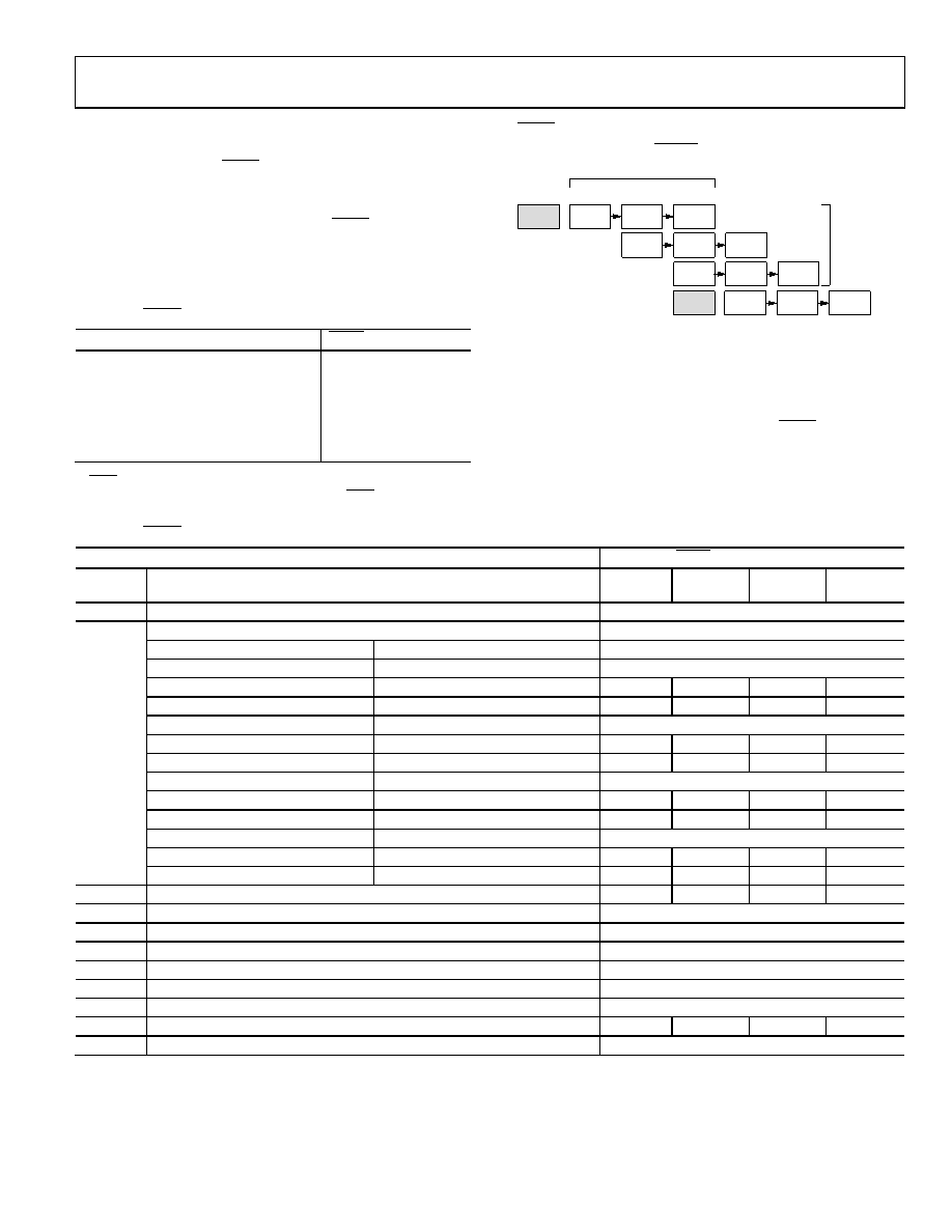
WRITE 1
FIRST
STAGE
SECOND
STAGE
THIRD
STAGE
~650ns
650ns
CALIBRATION ENGINE TIME
FOR EXAMPLE,
WRITE TO 3 FIN
DAC REGISTERS
350ns
WRITE 2
FIRST
STAGE
SECOND
STAGE
THIRD
STAGE
FIRST
STAGE
SECOND
STAGE
THIRD
STAGE
FIRST
STAGE
SECOND
STAGE
THIRD
STAGE
06197-
035
Figure 56. Multiple Writes to DAC X1 Registers
Writing data to the system control register, some PMU control
bits (see Table 18), the M register, and the C register do not
involve the digital calibration engine, thus speeding up
configuration of the device on power-on. However, care should
be taken not to issue these commands while BUSY is low, as
previously described.
Table 18. BUSY Pulse Widths for PMU Register Updates
PMU Register Update (See
Maximum BUSY Low Time per Channel Update
Bit
Bit Name
One
Channel
Two
Channels
Three
Channels
Four
Channels
21
CH EN
270 ns
20, 19
FORCE1, FORCE0 (depends on mode change)
Transition From
Transition To
High-Z FOHx current (11)
Force current (01)
270 ns
High-Z FOHx current (11)
Force voltage (00)
1.65 s
2.3 s
2.95 s
3.6 s
High-Z FOHx current (11)
High-Z FOHx voltage (10)
1.65 s
2.3 us
2.95 us
3.6 s
Force current (01)
High-Z FOHx current (11)
270 ns
Force current (01)
High-Z FOHx voltage (10)
1.65 s
2.3 s
2.95 s
3.6 s
Force current (01)
Force voltage (00)
1.65 s
2.3 s
2.95 s
3.6 s
High-Z FOHx voltage (10)
Force voltage (00)
270 ns
High-Z FOHx voltage (10)
Force current (01)
1.65 s
2.3 s
2.95 s
3.6 s
High-Z FOHx voltage (10)
High-Z FOHx current (11)
1.65 s
2.3 s
2.95 s
3.6 s
Force voltage (00)
High-Z FOHx voltage (10)
270 ns
Force voltage (00)
High-Z FOHx current (11)
1.65 s
2.3 s
2.95 s
3.6 s
Force voltage (00)
Force current (01)
1.65 s
2.3 s
2.95 s
3.6 s
17, 16, 15
C2 to C0; current range selection (any range change)
1.65 s
2.3 s
2.95 s
3.6 s
14, 13
MEASx (measure mode selection)
270 ns
12
FIN
270 ns
11
SFO
270 ns
10
SS0
270 ns
9
CL
270 ns
8
CPOLH
270 ns
7
Compare V/I
1.65 s
2.3 s
2.95 s
3.6 s
6
Clear
270 ns
相关PDF资料 |
PDF描述 |
|---|---|
| EVAL-AD5520EBZ | BOARD EVAL FOR AD5520 |
| MAX6198AESA+T | IC VREF SERIES PREC 4.096V 8SOIC |
| QPI-5-EVAL1 | EVALUATION BOARD FOR QPI-5 |
| H6MMH-4006M | DIP CABLE - HDM40H/AE40M/HDM40H |
| QPO-2-EVAL1 | EVALUATION BOARD FOR QPO-2 |
相关代理商/技术参数 |
参数描述 |
|---|---|
| EVAL-AD5522EBUZ | 功能描述:BOARD EVAL FOR 12X12MM AD5522 RoHS:是 类别:编程器,开发系统 >> 评估演示板和套件 系列:- 标准包装:1 系列:- 主要目的:电信,线路接口单元(LIU) 嵌入式:- 已用 IC / 零件:IDT82V2081 主要属性:T1/J1/E1 LIU 次要属性:- 已供物品:板,电源,线缆,CD 其它名称:82EBV2081 |
| EVAL-AD5532EB | 制造商:AD 制造商全称:Analog Devices 功能描述:32-Channel Infinite Sample-and-Hold |
| EVAL-AD5532EBZ | 功能描述:BOARD EVAL FOR AD5532 RoHS:是 类别:编程器,开发系统 >> 评估板 - 数模转换器 (DAC) 系列:- 产品培训模块:Lead (SnPb) Finish for COTS Obsolescence Mitigation Program 标准包装:1 系列:- DAC 的数量:4 位数:12 采样率(每秒):- 数据接口:串行,SPI? 设置时间:3µs DAC 型:电流/电压 工作温度:-40°C ~ 85°C 已供物品:板 已用 IC / 零件:MAX5581 |
| EVAL-AD5532HSEBZ | 功能描述:BOARD EVAL FOR AD5532HS RoHS:是 类别:编程器,开发系统 >> 评估板 - 数模转换器 (DAC) 系列:- 产品培训模块:Lead (SnPb) Finish for COTS Obsolescence Mitigation Program 标准包装:1 系列:- DAC 的数量:4 位数:12 采样率(每秒):- 数据接口:串行,SPI? 设置时间:3µs DAC 型:电流/电压 工作温度:-40°C ~ 85°C 已供物品:板 已用 IC / 零件:MAX5581 |
| EVAL-AD5533EB | 制造商:AD 制造商全称:Analog Devices 功能描述:32-Channel Precision Infinite Sample-and-Hold |
发布紧急采购,3分钟左右您将得到回复。