- 您现在的位置:买卖IC网 > PDF目录16871 > EVAL-AD5522EBDZ (Analog Devices Inc)BOARD EVAL FOR 14X14MM AD5522 PDF资料下载
参数资料
| 型号: | EVAL-AD5522EBDZ |
| 厂商: | Analog Devices Inc |
| 文件页数: | 57/64页 |
| 文件大小: | 0K |
| 描述: | BOARD EVAL FOR 14X14MM AD5522 |
| 标准包装: | 1 |
| 主要目的: | 测试与测量,参数测量单元(PMU) |
| 已用 IC / 零件: | AD5522 |
| 已供物品: | 板 |
第1页第2页第3页第4页第5页第6页第7页第8页第9页第10页第11页第12页第13页第14页第15页第16页第17页第18页第19页第20页第21页第22页第23页第24页第25页第26页第27页第28页第29页第30页第31页第32页第33页第34页第35页第36页第37页第38页第39页第40页第41页第42页第43页第44页第45页第46页第47页第48页第49页第50页第51页第52页第53页第54页第55页第56页当前第57页第58页第59页第60页第61页第62页第63页第64页
AD5522
Data Sheet
Rev. E | Page 60 of 64
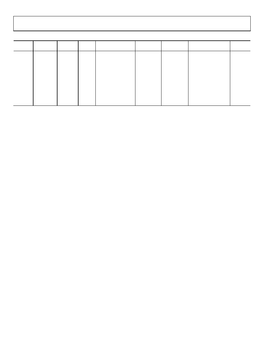
Table 39. ADCs and ADC Drivers Suggested For Use with AD55221
Part No.
Resolution
Sample
Rate
Ch. No.
AIN Range
Interface
ADC Driver
Multiplexer2
Package
16
250 kSPS
1
0 V to VREF
Serial, SPI
MSOP,
LFCSP
16
500 kSPS
1
0 V to VREF
Serial, SPI
MSOP,
LFCSP
16
500 kSPS
1
VREF to +VREF
Serial, SPI
MSOP,
LFCSP
16
250 kSPS
1
Bipolar 10 V, Bipolar
5 V, Unipolar 10 V,
Unipolar 5 V
Serial/Parallel
LFCSP,
LQFP
16
1 MSPS
4
0 V to 5 V
Serial/Parallel
1
Subset of the possible ADCs suitable for use with the AD5522. Visit www.analog.com for more options.
2
For purposes of sharing an ADC among multiple PMU channels. Note that the multiplexer is not absolutely necessary because the AD5522 MEASOUTx path has a tri-
state mode per channel.
3
Do not allow the MEASOUTx output range to exceed the analog input (AIN) range of the ADC.
POWER SUPPLY DECOUPLING
Careful consideration of the power supply and ground return
layout helps to ensure the rated performance. Design the
printed circuit board (PCB) on which the AD5522 is mounted
so that the analog and digital sections are separated and
confined to certain areas of the board. If the AD5522 is in a
system where multiple devices require an AGND-to-DGND
connection, the connection should be made at one point only.
Establish the star ground point as close as possible to the device.
For supplies with multiple pins (AVSS and AVDD), it is
recommended that these pins be tied together and that each
supply be decoupled only once.
The AD5522 should have ample supply decoupling of 10 F
in parallel with 0.1 F on each supply located as close to the
package as possible, ideally right up against the device. The
10 F capacitors are the tantalum bead type. The 0.1 F capac-
itors should have low effective series resistance (ESR) and low
effective series inductance (ESL)—typical of the common
ceramic types that provide a low impedance path to ground at
high frequencies—to handle transient currents due to internal
logic switching.
Avoid running digital lines under the device because they can
couple noise onto the device. However, allow the analog ground
plane to run under the AD5522 to avoid noise coupling (applies
only to the package with paddle up). The power supply lines of
the AD5522 should use as large a trace as possible to provide
low impedance paths and reduce the effects of glitches on the
power supply line. Fast switching digital signals should be
shielded with digital ground to avoid radiating noise to other
parts of the board, and they should never be run near the refer-
ence inputs. It is essential to minimize noise on all VREF lines.
Avoid crossover of digital and analog signals. Traces on opposite
sides of the board should run at right angles to each other to
reduce the effects of feedthrough through the board. As is the
case for all thin packages, care must be taken to avoid flexing
the package and to avoid a point load on the surface of this
package during the assembly process.
Also, note that the exposed paddle of the AD5522 is connected
to the negative supply, AVSS.
POWER SUPPLY SEQUENCING
When the supplies are connected to the AD5522, it is important
that the AGND and DGND pins be connected to the relevant
ground planes before the positive or negative supplies are applied.
This is the only power sequencing requirement for this device.
TYPICAL APPLICATION FOR THE AD5522
Figure 59 shows the AD5522 used in an ATE system. The device
can be used as a per-pin parametric unit to speed up the rate at
which testing can be done.
The central PMU (shown in the block diagram) is usually a
highly accurate PMU and is shared among a number of pins
in the tester. In general, many discrete levels are required in an
ATE system for the pin drivers, comparators, clamps, and active
loads. DAC devices such as the AD537x family offer a highly
integrated solution for a number of these levels.
相关PDF资料 |
PDF描述 |
|---|---|
| EVAL-AD5520EBZ | BOARD EVAL FOR AD5520 |
| MAX6198AESA+T | IC VREF SERIES PREC 4.096V 8SOIC |
| QPI-5-EVAL1 | EVALUATION BOARD FOR QPI-5 |
| H6MMH-4006M | DIP CABLE - HDM40H/AE40M/HDM40H |
| QPO-2-EVAL1 | EVALUATION BOARD FOR QPO-2 |
相关代理商/技术参数 |
参数描述 |
|---|---|
| EVAL-AD5522EBUZ | 功能描述:BOARD EVAL FOR 12X12MM AD5522 RoHS:是 类别:编程器,开发系统 >> 评估演示板和套件 系列:- 标准包装:1 系列:- 主要目的:电信,线路接口单元(LIU) 嵌入式:- 已用 IC / 零件:IDT82V2081 主要属性:T1/J1/E1 LIU 次要属性:- 已供物品:板,电源,线缆,CD 其它名称:82EBV2081 |
| EVAL-AD5532EB | 制造商:AD 制造商全称:Analog Devices 功能描述:32-Channel Infinite Sample-and-Hold |
| EVAL-AD5532EBZ | 功能描述:BOARD EVAL FOR AD5532 RoHS:是 类别:编程器,开发系统 >> 评估板 - 数模转换器 (DAC) 系列:- 产品培训模块:Lead (SnPb) Finish for COTS Obsolescence Mitigation Program 标准包装:1 系列:- DAC 的数量:4 位数:12 采样率(每秒):- 数据接口:串行,SPI? 设置时间:3µs DAC 型:电流/电压 工作温度:-40°C ~ 85°C 已供物品:板 已用 IC / 零件:MAX5581 |
| EVAL-AD5532HSEBZ | 功能描述:BOARD EVAL FOR AD5532HS RoHS:是 类别:编程器,开发系统 >> 评估板 - 数模转换器 (DAC) 系列:- 产品培训模块:Lead (SnPb) Finish for COTS Obsolescence Mitigation Program 标准包装:1 系列:- DAC 的数量:4 位数:12 采样率(每秒):- 数据接口:串行,SPI? 设置时间:3µs DAC 型:电流/电压 工作温度:-40°C ~ 85°C 已供物品:板 已用 IC / 零件:MAX5581 |
| EVAL-AD5533EB | 制造商:AD 制造商全称:Analog Devices 功能描述:32-Channel Precision Infinite Sample-and-Hold |
发布紧急采购,3分钟左右您将得到回复。