- 您现在的位置:买卖IC网 > PDF目录16871 > EVAL-AD5522EBDZ (Analog Devices Inc)BOARD EVAL FOR 14X14MM AD5522 PDF资料下载
参数资料
| 型号: | EVAL-AD5522EBDZ |
| 厂商: | Analog Devices Inc |
| 文件页数: | 64/64页 |
| 文件大小: | 0K |
| 描述: | BOARD EVAL FOR 14X14MM AD5522 |
| 标准包装: | 1 |
| 主要目的: | 测试与测量,参数测量单元(PMU) |
| 已用 IC / 零件: | AD5522 |
| 已供物品: | 板 |
第1页第2页第3页第4页第5页第6页第7页第8页第9页第10页第11页第12页第13页第14页第15页第16页第17页第18页第19页第20页第21页第22页第23页第24页第25页第26页第27页第28页第29页第30页第31页第32页第33页第34页第35页第36页第37页第38页第39页第40页第41页第42页第43页第44页第45页第46页第47页第48页第49页第50页第51页第52页第53页第54页第55页第56页第57页第58页第59页第60页第61页第62页第63页当前第64页
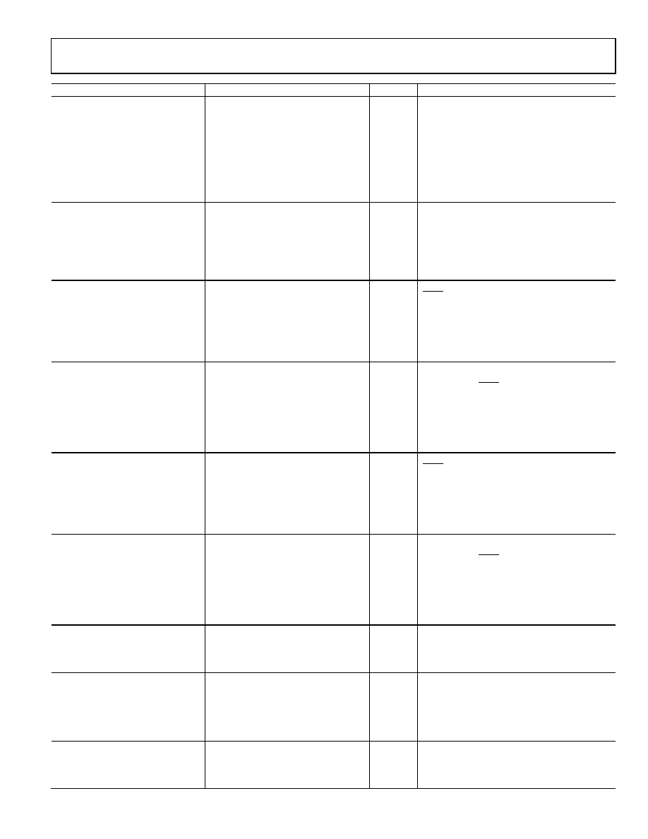
Data Sheet
AD5522
Rev. E | Page 9 of 64
Parameter
Min
Typ 1
Max
Unit
Test Conditions/Comments
GUARDx PIN
Output Voltage Span
22.5
V
Output Offset
10
+10
mV
Short-Circuit Current
15
+15
mA
Maximum Load Capacitance2
100
nF
Output Impedance
85
Ω
Tristate Leakage Current2
30
+30
nA
When guard amplifier is disabled
Slew Rate2
5
V/μs
CLOAD = 10 pF
Alarm Activation Time2
200
μs
Alarm delayed to eliminate false alarms
FORCE AMPLIFIER2
Slew Rate
0.4
V/μs
CCOMPx = 100 pF, CFFx = 220 pF, CLOAD = 200 pF
Gain Bandwidth
1.3
MHz
CCOMPx = 100 pF, CFFx = 220 pF, CLOAD = 200 pF
Max Stable Load Capacitance
10,000
pF
CCOMPx = 100 pF, larger CLOAD requires larger CCOMP
capacitor
100
nF
CCOMPx = 1 nF, larger CLOAD requires larger CCOMP
capacitor
FV SETTLING TIME TO 0.05% OF FS2
Midscale to full-scale change; measured from
SYNC rising edge, clamps on
±80 mA Range
22
40
s
CCOMPx = 100 pF, CFFx = 220 pF, CLOAD = 200 pF
±2 mA Range
24
40
s
CCOMPx = 100 pF, CFFx = 220 pF, CLOAD = 200 pF
±200 A Range
40
80
s
CCOMPx = 100 pF, CFFx = 220 pF, CLOAD = 200 pF
±20 A Range
300
s
CCOMPx = 100 pF, CFFx = 220 pF, CLOAD = 200 pF
±5 A Range
1400
s
CCOMPx = 100 pF, CFFx = 220 pF, CLOAD = 200 pF
MI SETTLING TIME TO 0.05% OF FS2
Midscale to full-scale change; driven from force
amplifier in FV mode, so includes FV settling time;
measured from SYNC rising edge, clamps on
±80 mA Range
22
40
s
CCOMPx = 100 pF, CFFx = 220 pF, CLOAD = 200 pF
±2 mA Range
24
40
s
CCOMPx = 100 pF, CFFx = 220 pF, CLOAD = 200 pF
±200 A Range
60
100
s
CCOMPx = 100 pF, CFFx = 220 pF, CLOAD = 200 pF
±20 A Range
462
s
CCOMPx = 100 pF, CFFx = 220 pF, CLOAD = 200 pF
±5 A Range
1902
s
CCOMPx = 100 pF, CFFx = 220 pF, CLOAD = 200 pF
FI SETTLING TIME TO 0.05% OF FS2
Midscale to full-scale change; measured from
SYNC rising edge, clamps on
±80 mA Range
24
55
s
CCOMPx = 100 pF, CLOAD = 200 pF
±2 mA Range
24
60
s
CCOMPx = 100 pF, CLOAD = 200 pF
±200 A Range
50
120
s
CCOMPx = 100 pF, CLOAD = 200 pF
±20 A Range
450
s
CCOMPx = 100 pF, CLOAD = 200 pF
±5 A Range
2700
s
CCOMPx = 100 pF, CLOAD = 200 pF
MV SETTLING TIME TO 0.05% OF FS2
Midscale to full-scale change; driven from force
amplifier in FV mode, so includes FV settling time;
measured from SYNC rising edge, clamps on
±80 mA Range
24
55
s
CCOMPx = 100 pF, CLOAD = 200 pF
±2 mA Range
24
60
s
CCOMPx = 100 pF, CLOAD = 200 pF
±200 A Range
50
120
s
CCOMPx = 100 pF, CLOAD = 200 pF
±20 A Range
450
s
CCOMPx = 100 pF, CLOAD = 200 pF
±5 A Range
2700
s
CCOMPx = 100 pF, CLOAD = 200 pF
DAC SPECIFICATIONS
Resolution
16
Bits
Output Voltage Span2
22.5
V
VREF = 5 V, within a range of 16.25 V to +22.5 V
Differential Nonlinearity2
1
+1
LSB
Guaranteed monotonic by design over temperature
COMPARATOR DAC DYNAMIC
SPECIFICATIONS2
Output Voltage Settling Time
1
s
500 mV change to ± LSB
Slew Rate
5.5
V/s
Digital-to-Analog Glitch Energy
20
nV-sec
Glitch Impulse Peak Amplitude
10
mV
REFERENCE INPUT
VREF DC Input Impedance
1
100
MΩ
VREF Input Current
10
+0.03
+10
A
VREF Range2
2
5
V
相关PDF资料 |
PDF描述 |
|---|---|
| EVAL-AD5520EBZ | BOARD EVAL FOR AD5520 |
| MAX6198AESA+T | IC VREF SERIES PREC 4.096V 8SOIC |
| QPI-5-EVAL1 | EVALUATION BOARD FOR QPI-5 |
| H6MMH-4006M | DIP CABLE - HDM40H/AE40M/HDM40H |
| QPO-2-EVAL1 | EVALUATION BOARD FOR QPO-2 |
相关代理商/技术参数 |
参数描述 |
|---|---|
| EVAL-AD5522EBUZ | 功能描述:BOARD EVAL FOR 12X12MM AD5522 RoHS:是 类别:编程器,开发系统 >> 评估演示板和套件 系列:- 标准包装:1 系列:- 主要目的:电信,线路接口单元(LIU) 嵌入式:- 已用 IC / 零件:IDT82V2081 主要属性:T1/J1/E1 LIU 次要属性:- 已供物品:板,电源,线缆,CD 其它名称:82EBV2081 |
| EVAL-AD5532EB | 制造商:AD 制造商全称:Analog Devices 功能描述:32-Channel Infinite Sample-and-Hold |
| EVAL-AD5532EBZ | 功能描述:BOARD EVAL FOR AD5532 RoHS:是 类别:编程器,开发系统 >> 评估板 - 数模转换器 (DAC) 系列:- 产品培训模块:Lead (SnPb) Finish for COTS Obsolescence Mitigation Program 标准包装:1 系列:- DAC 的数量:4 位数:12 采样率(每秒):- 数据接口:串行,SPI? 设置时间:3µs DAC 型:电流/电压 工作温度:-40°C ~ 85°C 已供物品:板 已用 IC / 零件:MAX5581 |
| EVAL-AD5532HSEBZ | 功能描述:BOARD EVAL FOR AD5532HS RoHS:是 类别:编程器,开发系统 >> 评估板 - 数模转换器 (DAC) 系列:- 产品培训模块:Lead (SnPb) Finish for COTS Obsolescence Mitigation Program 标准包装:1 系列:- DAC 的数量:4 位数:12 采样率(每秒):- 数据接口:串行,SPI? 设置时间:3µs DAC 型:电流/电压 工作温度:-40°C ~ 85°C 已供物品:板 已用 IC / 零件:MAX5581 |
| EVAL-AD5533EB | 制造商:AD 制造商全称:Analog Devices 功能描述:32-Channel Precision Infinite Sample-and-Hold |
发布紧急采购,3分钟左右您将得到回复。