- 您现在的位置:买卖IC网 > PDF目录16871 > EVAL-AD5522EBDZ (Analog Devices Inc)BOARD EVAL FOR 14X14MM AD5522 PDF资料下载
参数资料
| 型号: | EVAL-AD5522EBDZ |
| 厂商: | Analog Devices Inc |
| 文件页数: | 31/64页 |
| 文件大小: | 0K |
| 描述: | BOARD EVAL FOR 14X14MM AD5522 |
| 标准包装: | 1 |
| 主要目的: | 测试与测量,参数测量单元(PMU) |
| 已用 IC / 零件: | AD5522 |
| 已供物品: | 板 |
第1页第2页第3页第4页第5页第6页第7页第8页第9页第10页第11页第12页第13页第14页第15页第16页第17页第18页第19页第20页第21页第22页第23页第24页第25页第26页第27页第28页第29页第30页当前第31页第32页第33页第34页第35页第36页第37页第38页第39页第40页第41页第42页第43页第44页第45页第46页第47页第48页第49页第50页第51页第52页第53页第54页第55页第56页第57页第58页第59页第60页第61页第62页第63页第64页
Data Sheet
AD5522
Rev. E | Page 37 of 64
The calibration engine is engaged only when data is written to
the X1 register and for some PMU writes (see Table 18). The
calibration engine is not engaged when data is written to the M
or C register. This has the advantage of minimizing the initial
setup time of the device. To calculate a result that includes new
M or C data, a write to X1 is required.
CACHED X2 REGISTERS
Each DAC has a number of cached X2 registers. These registers
store the result of a gain and offset calibration in advance of a mode
change. This enables the user to preload registers, allowing the
calibration engine to calculate the appropriate X2 value and store
it until a change in mode occurs. Because the data is ready and
held in the appropriate register, mode changing is as time efficient
as possible. If an update occurs to a DAC register set that is
currently part of the operating PMU mode, the DAC output is
updated immediately (depending on the LOAD condition).
Gain and Offset Registers for the FIN DAC
The force amplifier input (FIN) DAC level contains independent
gain and offset control registers that allow the user to digitally
trim gain and offset. There are six sets of X1, M, and C registers:
one set for the force voltage range and one set for each force
current range (four internal current ranges and one external
current range). Six X2 registers store the calculated DAC values,
ready to load to the DAC register upon a PMU mode change.
SERIAL I/F
FIN
16
X1 REG
C REG
M REG
×6
16
16-BIT
FIN DAC
OFFSET DAC
X2 REG
VREF
06197-
030
Figure 51. FIN DAC Registers
Gain and Offset Registers for the Comparator DACs
The comparator DAC levels contain independent gain and
offset control registers that allow the user to digitally trim gain
and offset. There are six sets of X1, M, and C registers: one set
for the force voltage mode and one set for each force current
range (four internal current ranges and one external current
range). In this way, X2 can be preprogrammed, which allows for
efficient switching into the required compare mode. Six X2
registers store the calculated DAC values, ready to load to the
DAC register upon a PMU mode change.
SERIAL I/F
CPL
16
X1 REG
C REG
M REG
×6
16
16-BIT
CPL DAC
X2 REG
VREF
CPH
16
X1 REG
C REG
M REG
×6
16
16-BIT
CPH DAC
X2 REG
06197-
031
Figure 52. Comparator Registers
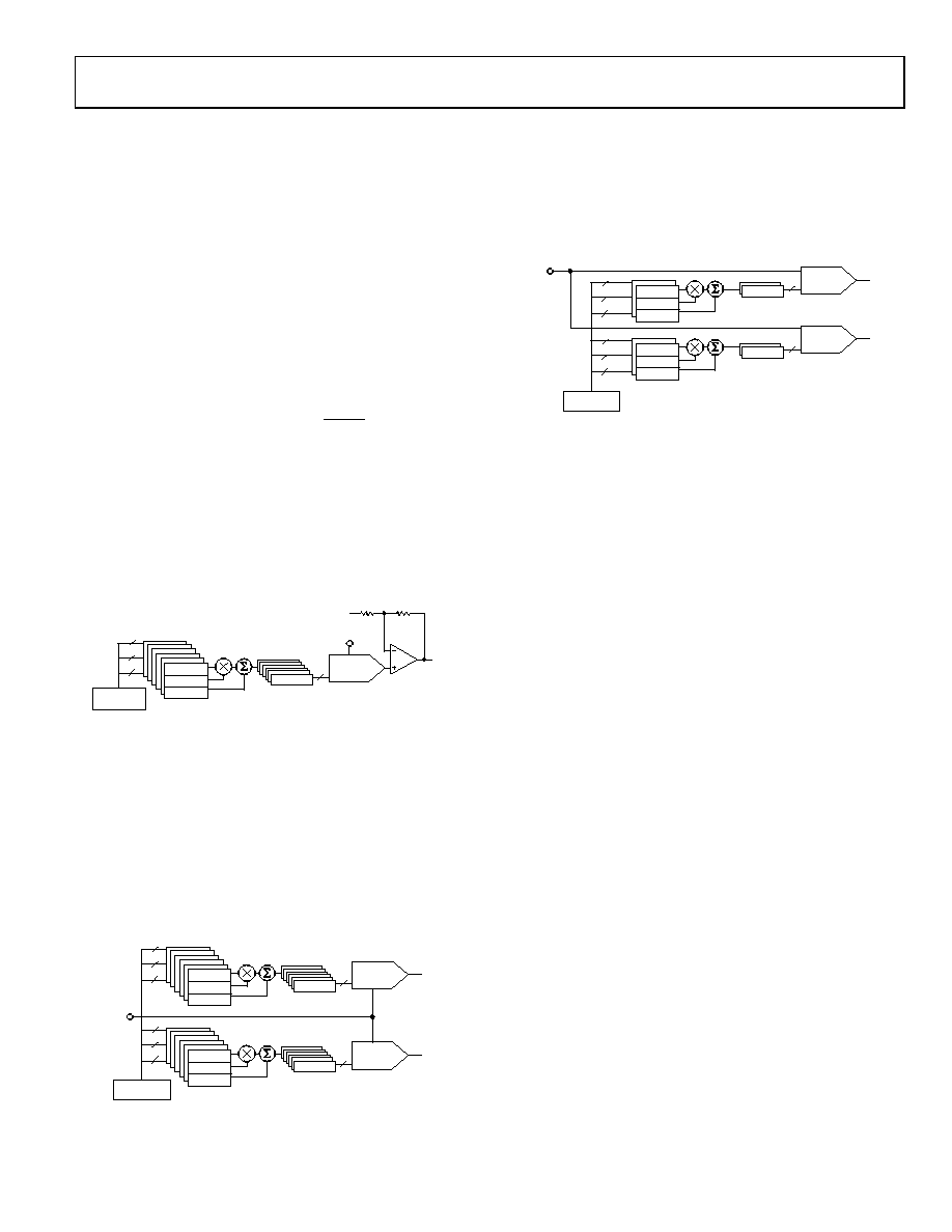
Gain and Offset Registers for the Clamp DACs
The clamp DAC levels contain independent gain and offset
control registers that allow the user to digitally trim gain and
offset. There are two sets of X1, M, and C registers: one set for
the force voltage mode and one set for all five current ranges.
Two X2 registers store the calculated DAC values, ready to load
to the DAC register upon a PMU mode change.
SERIAL I/F
CLL
16
X1 REG
C REG
M REG
16
16-BIT
CLL DAC
X2 REG
VREF
CLH
16
X1 REG
C REG
M REG
16
16-BIT
CLH DAC
X2 REG
06197-
032
×2
Figure 53. Clamp Registers
REFERENCE VOLTAGE (VREF)
One buffered analog input, VREF, supplies all 21 DACs with the
necessary reference voltage to generate the required dc levels.
REFERENCE SELECTION
The voltage applied to the VREF pin determines the output
voltage range and span applied to the force amplifier, clamp, and
comparator inputs. The AD5522 can be used with a reference
input ranging from 2 V to 5 V; however, for most applications,
a reference input of 5 V or 2.5 V is sufficient to meet all voltage
range requirements. The DAC amplifier gain is 4.5, which gives
a DAC output span of 22.5 V. The DACs have gain and offset
registers that can be used to trim out system errors.
In addition, the gain register can be used to reduce the DAC
output range to the desired force voltage range. The FIN DAC
retains 16-bit resolution even with a gain register setting of
quarter scale (0x4000). Therefore, from a single 5 V reference,
it is possible to obtain a voltage span as high as 22.5 V or as low
as 5.625 V.
When using the gain and offset registers, the selected output
range should take into account the system gain and offset errors
that need to be trimmed out. Therefore, the selected output
range should be larger than the actual required range.
When using low supply voltages, ensure that there is sufficient
headroom and footroom for the required force voltage range.
Also, the forced current range is the quoted full-scale range only
with an applied reference of 5 V (ISENSE amplifier gain = 10) or
2.5 V (ISENSE amplifier gain = 5).
相关PDF资料 |
PDF描述 |
|---|---|
| EVAL-AD5520EBZ | BOARD EVAL FOR AD5520 |
| MAX6198AESA+T | IC VREF SERIES PREC 4.096V 8SOIC |
| QPI-5-EVAL1 | EVALUATION BOARD FOR QPI-5 |
| H6MMH-4006M | DIP CABLE - HDM40H/AE40M/HDM40H |
| QPO-2-EVAL1 | EVALUATION BOARD FOR QPO-2 |
相关代理商/技术参数 |
参数描述 |
|---|---|
| EVAL-AD5522EBUZ | 功能描述:BOARD EVAL FOR 12X12MM AD5522 RoHS:是 类别:编程器,开发系统 >> 评估演示板和套件 系列:- 标准包装:1 系列:- 主要目的:电信,线路接口单元(LIU) 嵌入式:- 已用 IC / 零件:IDT82V2081 主要属性:T1/J1/E1 LIU 次要属性:- 已供物品:板,电源,线缆,CD 其它名称:82EBV2081 |
| EVAL-AD5532EB | 制造商:AD 制造商全称:Analog Devices 功能描述:32-Channel Infinite Sample-and-Hold |
| EVAL-AD5532EBZ | 功能描述:BOARD EVAL FOR AD5532 RoHS:是 类别:编程器,开发系统 >> 评估板 - 数模转换器 (DAC) 系列:- 产品培训模块:Lead (SnPb) Finish for COTS Obsolescence Mitigation Program 标准包装:1 系列:- DAC 的数量:4 位数:12 采样率(每秒):- 数据接口:串行,SPI? 设置时间:3µs DAC 型:电流/电压 工作温度:-40°C ~ 85°C 已供物品:板 已用 IC / 零件:MAX5581 |
| EVAL-AD5532HSEBZ | 功能描述:BOARD EVAL FOR AD5532HS RoHS:是 类别:编程器,开发系统 >> 评估板 - 数模转换器 (DAC) 系列:- 产品培训模块:Lead (SnPb) Finish for COTS Obsolescence Mitigation Program 标准包装:1 系列:- DAC 的数量:4 位数:12 采样率(每秒):- 数据接口:串行,SPI? 设置时间:3µs DAC 型:电流/电压 工作温度:-40°C ~ 85°C 已供物品:板 已用 IC / 零件:MAX5581 |
| EVAL-AD5533EB | 制造商:AD 制造商全称:Analog Devices 功能描述:32-Channel Precision Infinite Sample-and-Hold |
发布紧急采购,3分钟左右您将得到回复。