- 您现在的位置:买卖IC网 > PDF目录16560 > EVAL-ADF4193EBZ2 (Analog Devices Inc)BOARD EVALUATION EB2 FOR ADF4193 PDF资料下载
参数资料
| 型号: | EVAL-ADF4193EBZ2 |
| 厂商: | Analog Devices Inc |
| 文件页数: | 4/32页 |
| 文件大小: | 0K |
| 描述: | BOARD EVALUATION EB2 FOR ADF4193 |
| 标准包装: | 1 |
| 主要目的: | 计时,频率合成器 |
| 嵌入式: | 否 |
| 已用 IC / 零件: | ADF4193 |
| 主要属性: | 400 MHz ~ 3.5 GHz,数字式可编程输出相位 |
| 次要属性: | 板不包括环路滤波器和 VCO |
| 已供物品: | 板,缆线,CD |
| 相关产品: | ADF4193BCPZ-ND - IC PLL FREQ SYNTHESIZER 32LFCSP ADF4193BCPZ-RL7-ND - IC PLL FREQ SYNTHESIZER 32LFCSP ADF4193BCPZ-RL-ND - IC PLL FREQ SYNTHESIZER 32LFCSP |
第1页第2页第3页当前第4页第5页第6页第7页第8页第9页第10页第11页第12页第13页第14页第15页第16页第17页第18页第19页第20页第21页第22页第23页第24页第25页第26页第27页第28页第29页第30页第31页第32页
ADF4193
Data Sheet
Rev. F | Page 12 of 32
The value of MOD is chosen to give the desired channel step
with the available reference frequency. Thereafter, program the
INT and FRAC words for the desired RF output frequency. See
the Worked Example section for more information.
PFD and Charge Pump
The PFD takes inputs from the R divider and N divider and
produces up and down outputs with a pulse width difference
proportional to the phase difference between the inputs. The
charge pump outputs a net up or down current pulse of a width
equal to this difference, to pump up or pump down the voltage
that is integrated onto the loop filter, which in turn increases or
decreases the VCO output frequency. If the N divider phase lags
the R divider phase, a net up current pulse is produced that
increases the VCO frequency (and thus the phase). If the N
divider phase leads the R divider edge, then a net down pulse is
produced to reduce the VCO frequency and phase. Figure 23 is
a simplified schematic of the PFD and charge pump. The charge
pump is made up of an array of 64 identical cells, each of which
is fully differential. All 64 cells are active during fast lock, but
only one is active during normal operation. Because a single-
ended control voltage is required to tune the VCO, an on-chip,
differential-to-single-ended amplifier is provided for this purpose.
In addition, because the phase-lock loop only controls the
differential voltage generated across the charge pump outputs,
an internal common-mode feedback (CMFB) loop biases the
charge pump outputs at a common-mode voltage of approximately
2 V.
05328-019
CLR
Q
D
R DIVIDER
N DIVIDER
CHARGE
PUMP
ARRAY
[64:1]
CMFB
EN[64:1]
CLR
Q
D
CPOUT+
CPOUT–
Figure 23. PFD and Differential Charge Pump Simplified Schematic
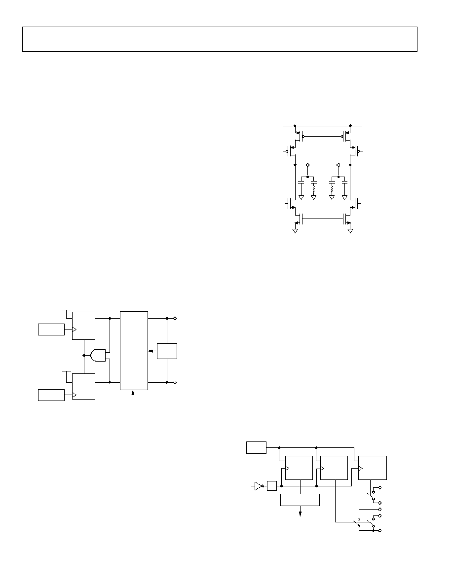
Differential Charge Pump
The charge pump cell (see Figure 24) has a fully differential
design for best up-to-down current matching. Good matching
is essential to minimize the phase offset created when switching
the charge pump current from its high value (in fast lock mode)
to its nominal value (in normal mode).
To pump up, the up switches are on and PMOS current is
sourced out through CPOUT+; this increases the voltage on the
external loop filter capacitors connected to CPOUT+. Similarly,
the NMOS current sink on CPOUT decreases the voltage on the
external loop filter capacitors connected to CPOUT. Therefore,
the differential voltage between CPOUT+ and CPOUT increases.
To pump down, PMOS current sources out through CPOUT and
NMOS current sinks in through CPOUT+, which decreases the
(CPOUT+, CPOUT) differential voltage. The charge pump up/
down matching is improved by an order of magnitude over the
conventional single-ended charge pump that depended on the
matching of two different device types. The up/down matching
in this structure depends on how a PMOS matches a PMOS and
an NMOS matches an NMOS.
05328-035
VBIAS P
P
N
UP
DOWN
UP
VBIAS N
CPOUT+
CPOUT–
Figure 24. Differential Charge Pump Cell with External Loop Filter Components
Fast Lock Timeout Counters
Timeout counters, clocked at one quarter the PFD reference
frequency, are provided to precisely control the fast locking
operation (see Figure 25). Whenever a new frequency is
programmed, the fast lock timers start and the PLL locks into
wide BW mode with the 64 identical 100 A charge pump cells
active (6.4 mA total). When the ICP counter times out, the
charge pump current is reduced to 1× by deselecting cells in
binary steps over the next six timer clock cycles, until just one
100 A cell is active. The charge pump current switching from
6.4 mA to 100 A equates to an 8-to-1 change in loop bandwidth.
The loop filter must be changed to ensure stability when this
happens. That is the job of the SW1, SW2, and SW3 switches. The
application circuit (shown in Figure 36) shows how they can be
used to reconfigure the loop filter time constants. The application
circuits close to short out external loop filter resistors during fast
lock and open when their counters time out to restore the filter
time constants to their normal values for the 100 A charge
pump current. Because it takes six timer clock cycles to reduce
the charge pump current to 1×, it is recommended that both
switch timers be programmed to the value of the ICP timer + 7.
05328-
036
SW1/SW2
TIMEOUT
COUNTER
SW3
TIMEOUT
COUNTER
ICP
TIMEOUT
COUNTER
EN[64:1]
÷4
START
FPFD
SW3
AOUT
SW2
SWGND
SW1
WRITE
TO R0
CHARGE PUMP
ENABLE LOGIC
Figure 25. Fast Lock Timeout Counters
相关PDF资料 |
PDF描述 |
|---|---|
| RMC06DRTH-S734 | CONN EDGECARD 12POS DIP .100 SLD |
| HBM18DSUN | CONN EDGECARD 36POS .156 DIP SLD |
| RSC06DREI-S734 | CONN EDGECARD 12POS .100 EYELET |
| EBA24DRMI | CONN EDGECARD 48POS .125 SQ WW |
| MAX8663ETL+T | IC PMIC LI+ SNGL CELL 40TQFN |
相关代理商/技术参数 |
参数描述 |
|---|---|
| EVAL-ADF4206-7EB1 | 制造商:Analog Devices 功能描述:EVALUATION BOARD FOR DUAL RF PLL FREQUENCY SYNTHESIZERS 制造商:Analog Devices 功能描述:DUAL RF PLL FREQ SYNTHESIZERS - Bulk |
| EVAL-ADF4208EB1 | 制造商:Analog Devices 功能描述:Evaluation Board For Dual RF PLL Frequency Synthesizers 制造商:Analog Devices 功能描述:DUAL RF PLL FREQ SYNTHESIZERS - Bulk |
| EVAL-ADF4212EB1 | 制造商:Analog Devices 功能描述:EVALUATION BOARD I.C. - Bulk |
| EVAL-ADF4213EB1 | 制造商:Analog Devices 功能描述:EVALUATION BOARD I.C. - Bulk |
| EVAL-ADF4213EB2 | 制造商:Analog Devices 功能描述:EVALUATION BOARD I.C. - Bulk |
发布紧急采购,3分钟左右您将得到回复。