- 您现在的位置:买卖IC网 > PDF目录371807 > HFA3824A (Intersil Corporation) Direct Sequence Spread Spectrum Baseband Processor PDF资料下载
参数资料
| 型号: | HFA3824A |
| 厂商: | Intersil Corporation |
| 元件分类: | 基带处理器 |
| 英文描述: | Direct Sequence Spread Spectrum Baseband Processor |
| 中文描述: | 直接序列扩频基带处理器 |
| 文件页数: | 28/40页 |
| 文件大小: | 271K |
| 代理商: | HFA3824A |
第1页第2页第3页第4页第5页第6页第7页第8页第9页第10页第11页第12页第13页第14页第15页第16页第17页第18页第19页第20页第21页第22页第23页第24页第25页第26页第27页当前第28页第29页第30页第31页第32页第33页第34页第35页第36页第37页第38页第39页第40页
2-126
CONFIGURATION REGISTER 3 ADDRESS (0Ch) MODEM CONFIGURATION REGISTER D
Bit 7
This bit determines when MD_RDY goes active on a good signal.
Logic 1 = After SFD
Logic 0 = After CRC
Bit 6, 5
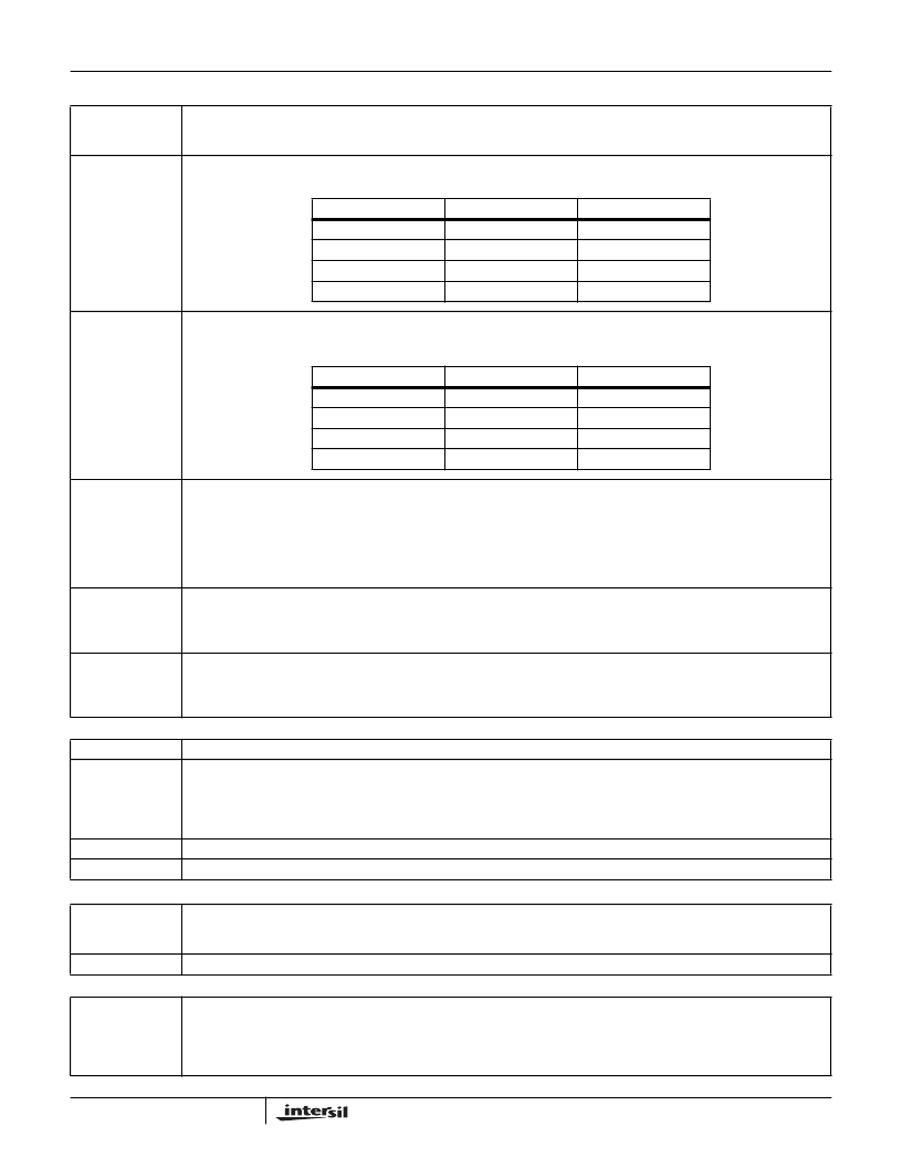
These control bits combined are used to select the number of chips per symbol used in the I and Q transmit paths (see table
below).
Bit 4, 3
These control bits are used to select the divide ratio for the transmit chip clock timing.
NOTE: The value of N is determined by the following equation: Symbol Rate = MCLK/(N x Chips per symbol). If N is set for
values of 4, 8 or 16, see TB361 for additional information.
Bit 2
This control bit is used to select the origination of Preamble/Header information.
Logic 1: The HFA3824A generates the Preamble and Header internally by formatting the programmed header
information and generating a TX_RDY to indicate the beginning of the data packet.
Logic 0: Accepts the Preamble/Header information from an externally generated source.
When external header is selected the HFA3824A will search the incoming data stream for a match to the SFD. Once the
SFD is found the transmit header mode selection then is used to determine the end of the header, (the point of rate switching,
if required).
Bit 1
This control bit is used to indicate the signal modulation type for the transmitted data packet. When configured for mode 0
header, or mode 3 and external header, this bit is ignored. See Register 0 bits 4 and 3.
Logic 1 = DBPSK modulation for data packet.
Logic 0 = DQPSK modulation for data packet.
Bit 0
This control bit is used to indicate the signal modulation type for the received data packet used only with header modes 1
and 2. See register 2 bits 1 and 0.
Logic 1 = DBPSK.
Logic 0 = DQPSK.
CHIPS PER
BIT 6
BIT 5
11
0
0
13
0
1
15
1
0
16
1
1
MASTER
BIT 4
BIT 3
N = 2
0
0
N = 4
0
1
N = 8
1
0
N = 16
1
1
CONFIGURATION REGISTER 4 ADDRESS (10h)
Bit 7
Reserved (must set to “0”)
Bit 6
Enable receiver reset if phase greater than 45 degrees between symbols. Useful in continuous QPSK mode to allow modem
to drop the link under interference conditions that would not degrade signal quality thresholds sufficiently to drop link but
would cause data errors. Also prevents receiver acquisition on off frequency signal sidelobes.
Logic 1 = Enabled
Logic 0 = Disable
Bit 4, 5
Reserved (must set to “0”)
Bit 3-0
See Table 5. Test Modes
CONFIGURATION REGISTER 5 ADDRESS (14h, 18h) INTERNAL TEST REGISTER B
Bit 7
Invert Q input to receiver.
0 = Normal
1 = Invert
Bits 6 - 0
These bits need to be programmed to 0h. They are used for manufacturing test only.
CONFIGURATION REGISTER 7 ADDRESS (1Ch) MODEM STATUS REGISTER A
Bit 7
This bit indicates the status of the TX_RDY output pin. TX_RDY is used only when the HFA3824A generates the Pream-
ble/Header data internally.
Logic 1: Indicates that the HFA3824A has completed transmitting Preamble header information and is ready to accept data
from the external source (i.e., MAC) to transmit.
Logic 0: Indicates that the HFA3824A is in the process of transmitting Preamble Header information.
HFA3824A
相关PDF资料 |
PDF描述 |
|---|---|
| HFA3842B | PCMCIA/USB Wireless LAN Medium Access Controller |
| HFA3842BIN | PCMCIA/USB Wireless LAN Medium Access Controller |
| HFA3842BIN-TK | PCMCIA/USB Wireless LAN Medium Access Controller |
| HFA3842IN96 | Wireless LAN Medium Access Controller |
| HFA3842 | Wireless LAN Medium Access Controller |
相关代理商/技术参数 |
参数描述 |
|---|---|
| HFA3824AIV | 制造商:Rochester Electronics LLC 功能描述:BASEBAND PROCESSOR - Bulk |
| HFA3824AIV WAF | 制造商:Harris Corporation 功能描述: |
| HFA3824AIV96 | 制造商:Rochester Electronics LLC 功能描述:BASEBAND PROCESSOR - Bulk |
| HFA3824EVAL | 制造商:Rochester Electronics LLC 功能描述:- Bulk |
| HFA3824IV | 制造商:Rochester Electronics LLC 功能描述:- Bulk |
发布紧急采购,3分钟左右您将得到回复。