- 您现在的位置:买卖IC网 > PDF目录67682 > IBM25PPC750-DB0M2500 32-BIT, 250 MHz, RISC PROCESSOR, CBGA360 PDF资料下载
参数资料
| 型号: | IBM25PPC750-DB0M2500 |
| 元件分类: | 微控制器/微处理器 |
| 英文描述: | 32-BIT, 250 MHz, RISC PROCESSOR, CBGA360 |
| 封装: | 25 X 25 MM, 1.27 MM PITCH, CERAMIC, BGA-360 |
| 文件页数: | 2/42页 |
| 文件大小: | 496K |
| 代理商: | IBM25PPC750-DB0M2500 |
第1页当前第2页第3页第4页第5页第6页第7页第8页第9页第10页第11页第12页第13页第14页第15页第16页第17页第18页第19页第20页第21页第22页第23页第24页第25页第26页第27页第28页第29页第30页第31页第32页第33页第34页第35页第36页第37页第38页第39页第40页第41页第42页
Page 10
v 3.2
Datasheet
7/15/99
PowerPC 750TM SCM RISC Microprocessor
Preliminary Copy
AC Electrical Characteristics
This section provides the AC electrical characteristics for the 750. After fabrication, parts are sorted by maxi-
mum processor core frequency as shown in Section , “Clock AC Specifications,” and tested for conformance
to the AC specifications for that frequency. These specifications are for 200, 225, 233, 250, 266, 275, and
300 MHz processor core frequencies. The processor core frequency is determined by the bus (SYSCLK) fre-
quency and the settings of the PLL_CFG(0-3) signals. Parts are sold by maximum processor core frequency
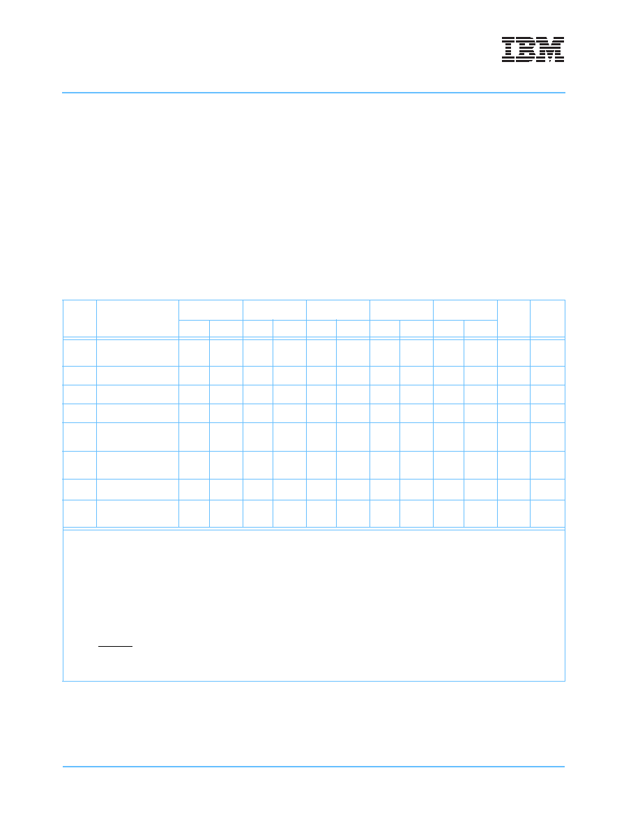
Clock AC Specications
Table 7.
Clock AC Timing Specications
See Table 2 for operating conditions.
Num
Characteristic
200 MHz
225/233 MHz
250/266 MHz
275 MHz
300 MHz
Unit
Notes
Min
Max
Min
Max
Min
Max
Min
Max
Min
Max
Processor
frequency
150
200
150
233
150
266
150
275
200
300
MHz
VCO frequency
300
400
300
466
300
533
300
550
400
600
MHz
SYSCLK frequency
25
83.3
25
83.3
25
83.3
25
83.3
25
100
MHz
1
SYSCLK cycle time
12
40
12
40
12
40
12
40
10
40
ns
2,3
SYSCLK rise and
fall time
—
2.0
—
2.0
—
2.0
—
2.0
—
2.0
ns
2,3
4
SYSCLK duty cycle
measured at 1.4 V
40
60
40
60
40
60
40
60
40
60
%
3
SYSCLK jitter
—
±150
—
±150
—
±150
—
±150
—
±150
ps
4,3
Internal PLL relock
time
—
100
—
100
—
100
—
100
—
100
s
5
Note:
1. Note: The SYSCLK frequency and the PLL_CFG[0-3] settings must be chosen such that the resulting SYSCLK (bus) fre-
quency, CPU (core) frequency, and PLL (VCO) frequency do not exceed their respective maximum or minimum operating
frequencies. Refer to the PLL_CFG[0-3] signal description in Section , “PLL Conguration,” for valid PLL_CFG[0-3] set-
tings.
2. Rise and fall times for the SYSCLK input are measured from 0.4 to 2.4V.
3. Timing is guaranteed by design and characterization, and is not tested.
4. The total input jitter (short term and long term combined) must be under
±150ps.
5. Relock timing is guaranteed by design and characterization, and is not tested. PLL-relock time is the maximum amount of
time required for PLL lock after a stable VDD and SYSCLK are reached during the power-on reset sequence. This speci-
cation also applies when the PLL has been disabled and subsequently re-enabled during sleep mode. Also note that
HRESET must be held asserted for a minimum of 255 bus clocks after the PLL-relock time during the power-on reset
sequence.
*
Subject to availability - see your marketing representative.
相关PDF资料 |
PDF描述 |
|---|---|
| IBM25PPC750CX-CP30-3T | 32-BIT, 433 MHz, RISC PROCESSOR, PBGA256 |
| IBM25PPC750CX-CP40-3T | 32-BIT, 466 MHz, RISC PROCESSOR, PBGA256 |
| IBM25PPC750CXEFP10-3T | RISC PROCESSOR, PBGA256 |
| IBM25PPC750CXEJP7012T | 32-BIT, 600 MHz, RISC PROCESSOR, PBGA256 |
| IBM25PPC750CXEJP5523T | 32-BIT, 533 MHz, RISC PROCESSOR, PBGA256 |
相关代理商/技术参数 |
参数描述 |
|---|---|
| IBM25PPC750FL-GR0123V | 制造商:IBM 功能描述:MPU 750XX RISC 32BIT - Trays |
| IBM25PPC750FL-GR0124V | 制造商:IBM 功能描述:MPU 750XX RISC 32BIT - Trays |
| IBM25PPC750FL-GR0133T | 制造商:IBM 功能描述:IBMIBM25PPC750FL-GR0133T CSOI9SG LOGIC P |
| IBM25PPC750FL-GR0133V | 制造商:IBM 功能描述:MPU 750XX RISC 32BIT - Trays |
| IBM25PPC750FL-GR1024T | 制造商:IBM 功能描述: |
发布紧急采购,3分钟左右您将得到回复。