- 您现在的位置:买卖IC网 > PDF目录67685 > ICS5342 PALETTE-DAC DSPL CTLR, PQCC68 PDF资料下载
参数资料
| 型号: | ICS5342 |
| 元件分类: | 显示控制器 |
| 英文描述: | PALETTE-DAC DSPL CTLR, PQCC68 |
| 封装: | PLASTIC, LCC-68 |
| 文件页数: | 10/36页 |
| 文件大小: | 1017K |
| 代理商: | ICS5342 |
第1页第2页第3页第4页第5页第6页第7页第8页第9页当前第10页第11页第12页第13页第14页第15页第16页第17页第18页第19页第20页第21页第22页第23页第24页第25页第26页第27页第28页第29页第30页第31页第32页第33页第34页第35页第36页

ICS5342
GENDAC
18
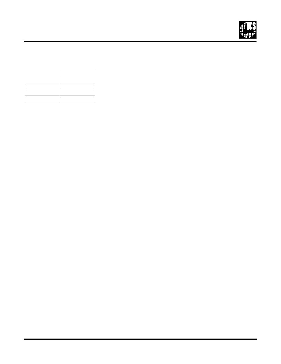
N2 Post Divide Code
If mode 4 is set in the command register, CR7-CR4 bits equal
0001, and the N2 code must be 10.
The block diagram of the PLL clock synthesizer is shown in
figure 3.
Based on the M and N values, the output frequency of the
clocks is given by the following equation:
M and N values should be programmed such that the frequen-
cy of the VC0 is within the optimum range for duty cycle, jit-
ter and glitch free transition. Optimum duty cycle is achieved
by programming N2 for values greater than unity. See the next
section for a programming example.
Programming Example
Suppose an output frequency of 25.175 MHz is desired. The
reference crystal is 14.318 MHz. The VCO should be targeted
to run in the 60 to 270 MHz range, so choosing a post divide
of 4 gives a VCO frequency of:
From the table in the previous section, we find N2 = 2 Substi-
tuting FREF = 14.318 and 2
N2 = 4 into the clock frequency
equation in the previous section:
By trial and error:
M + 2 = 127
M = 125
N1 + 2 = 18
N1 = 16
so the registers are:
M = 125d = 1 1 1 1 1 0 1 b
N = 0 & N2 code & N1 = 0 & 1 0 & 1 0 0 0 0
N = 0 1 0 1 0 0 0 0 b
Additional Information on Programming
the Frequency Generator section of the
GENDAC
When programming the GENDAC PLL parameter registers,
there are many possible combinations of parameters which
will give the correct output frequency. Some combinations are
better than others, however. Here is a method to determine
how the registers need to be set:
The key guidelines come from the operation of the phase
locked loop, which has the following restrictions:
1.
This refers to the input refer-
ence frequency. Most users simply connect a 14.318
MHz crystal to the crystal inputs, so this is not a prob-
lem.
2.
This is the frequency input to
the phase detector.
3.
This is the VCO
frequency. In general, the VCO should run as fast as pos-
sible, because it has lower jitter at higher frequencies.
Also, running the VCO at multiples of the desired fre-
quency allows the use of output divides, which tends to
improve the duty cycle.
4.
This is the output fre-
quency.
These rules lead to the following procedure for determining
the PLL parameters, assuming rules 1 and 4 are satisfied.
A. Determine the value of N2 (either 1, 2, 4 or 8) by select-
ing the highest value of N2, which satises the condition
N2* fCLK < 270 Mhz.
B. Calculate:
C. Now (M+2) and (N1+2) must be found by trial and error.
With a 14.318 MHz reference frequency, there will gen-
erally be a small output frequency error due to the reso-
lution limit of (M+2) and (N1+2). For a given frequency
tolerance, several different (M+2) and (N1+2) combina-
tions can usually be found. Usually, a few minutes trying
N2 Post Divide Code
N2 Code
Divider
00
1
01
2
10
4
11
8
F
OUT
M
2
+
()F
REF
2N2 N12
+
()
---------------------------------
=
4
25.175
×
101.021 MHz
=
25.175
14.318
---------------- 4
M
2
+
N12
+
-----------------
=
2 MHz
f
REF
25 MHz
<<
600KHz
f
REF
N12
+
-----------------
8MHz
≤≤
60MHz
M
2
+
N12
+
----------------- f
REF
270 MHz
≤≤
f
CLK 0 and f CLK 1
35 MHz
≤
M
2
+
N 12
+
-----------------
2N2 f
OUT
f
REF
-----------------------
=
相关PDF资料 |
PDF描述 |
|---|---|
| ICS552ARI-01LFT | 200 MHz, OTHER CLOCK GENERATOR, PDSO20 |
| ICS552R-01ILF | 200 MHz, OTHER CLOCK GENERATOR, PDSO20 |
| ICS557G-05ATR | 200 MHz, PROC SPECIFIC CLOCK GENERATOR, PDSO20 |
| ICS557G-08LF | 557 SERIES, LOW SKEW CLOCK DRIVER, 1 TRUE OUTPUT(S), 0 INVERTED OUTPUT(S), PDSO16 |
| ICS557G-08LFT | 557 SERIES, LOW SKEW CLOCK DRIVER, 1 TRUE OUTPUT(S), 0 INVERTED OUTPUT(S), PDSO16 |
相关代理商/技术参数 |
参数描述 |
|---|---|
| ICS5342-1 | 制造商:ICS 制造商全称:ICS 功能描述:Analog IC |
| ICS5342-2 | 制造商:ICS 制造商全称:ICS 功能描述:Analog IC |
| ICS5342-3 | 制造商:ICS 制造商全称:ICS 功能描述:Analog IC |
| ICS5342ADD | 制造商:ICS 制造商全称:ICS 功能描述:Addendum to ICS5342 Data Sheet |
| ICS5342V | 制造商:未知厂家 制造商全称:未知厂家 功能描述:Peripheral IC |
发布紧急采购,3分钟左右您将得到回复。