- 您现在的位置:买卖IC网 > PDF目录67685 > ICS5342 PALETTE-DAC DSPL CTLR, PQCC68 PDF资料下载
参数资料
| 型号: | ICS5342 |
| 元件分类: | 显示控制器 |
| 英文描述: | PALETTE-DAC DSPL CTLR, PQCC68 |
| 封装: | PLASTIC, LCC-68 |
| 文件页数: | 12/36页 |
| 文件大小: | 1017K |
| 代理商: | ICS5342 |
第1页第2页第3页第4页第5页第6页第7页第8页第9页第10页第11页当前第12页第13页第14页第15页第16页第17页第18页第19页第20页第21页第22页第23页第24页第25页第26页第27页第28页第29页第30页第31页第32页第33页第34页第35页第36页
ICS5342
GENDAC
2
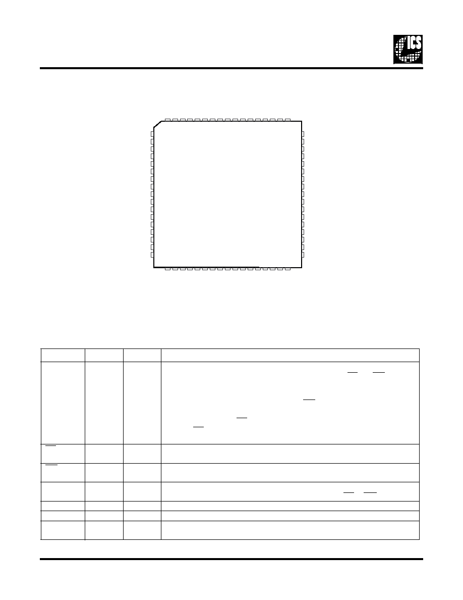
Pin Conguration
Pin Description (68-pin PLCC)
Symbol
Pin #
Type
Description
D7 - D0
21-14
I/O
Systems data bus bidirectional data I/O lines – used by host microprocessor for
internal register read and write operations (using active low RD and WR respec-
tively) for six internal registers: Pixel Address, Color Value, Pixel Mask, PLL
Address, PLL Parameter, and Command
During the write cycle, the rising edge of WR latches the data into the selected
register (set by the status of the three RS pins).
The rising edge of RD determines the end of the read cycle.
The RD set logical high indicates that data I/O lines no longer contain infor-
mation from the selected register and will be tri-stated.
RD
5
Input
RAM/PLL read enable bus control signal – in active low state, any information
present on the internal data bus is available on the Data I/O lines, D0-D7
WR
22
Input
Active low RAM/PLL write enable bus control signal – controls write timing on
microprocessor interface inputs, D0-D7
RS2-RS0
63,24,23
Input
Register address select 0 inputs – control selection of one of six internal registers –
inputs are sampled on falling edge of active enable signal (RD or WR)
XIN
48
Input
Crystal input – connect to 14.318 MHz crystal
XOUT
49
Output
Crystal output – connect to 14.318 MHz crystal
MSW
25
Input
Mode switch – digital control for selecting primary and secondary pixel color
modes – low selects primary mode – connect to ground if not used
AGND
N/C
RED
AVDD
CVDD
GRN
BLUE
RSET
DVDD
CGND
PCLK
P7
P6
P5
P4
P3
P2
P1
P0
XVDD
XGND
XOUT
XIN
VREF
N/C
DGND
5342_02
CLK0
P13
RD*
STROBE*
BLANK*
P9
CS1
CS0
P12
P11
CVDD
P10
P8
N/C
CVDD
SENSE*
36
35
34
33
32
31
30
29
28
27
40
39
38
37
43
42
41
60
59
58
57
56
55
54
53
52
51
50
49
48
47
46
45
44
1
2
3
4
5
6
7
8
9
68
64
65
66
67
61
62
63
GENDAC II
ICS5342
D0
D1
D2
D3
D4
D5
CGND
CLK1
P14
P15
WR*
RS0
RS1
MSW
CGND
10
11
12
13
14
15
16
17
18
19
20
21
22
23
24
25
26
D7
D6
RS2
ICS5342 (68-pin PLCC)
相关PDF资料 |
PDF描述 |
|---|---|
| ICS552ARI-01LFT | 200 MHz, OTHER CLOCK GENERATOR, PDSO20 |
| ICS552R-01ILF | 200 MHz, OTHER CLOCK GENERATOR, PDSO20 |
| ICS557G-05ATR | 200 MHz, PROC SPECIFIC CLOCK GENERATOR, PDSO20 |
| ICS557G-08LF | 557 SERIES, LOW SKEW CLOCK DRIVER, 1 TRUE OUTPUT(S), 0 INVERTED OUTPUT(S), PDSO16 |
| ICS557G-08LFT | 557 SERIES, LOW SKEW CLOCK DRIVER, 1 TRUE OUTPUT(S), 0 INVERTED OUTPUT(S), PDSO16 |
相关代理商/技术参数 |
参数描述 |
|---|---|
| ICS5342-1 | 制造商:ICS 制造商全称:ICS 功能描述:Analog IC |
| ICS5342-2 | 制造商:ICS 制造商全称:ICS 功能描述:Analog IC |
| ICS5342-3 | 制造商:ICS 制造商全称:ICS 功能描述:Analog IC |
| ICS5342ADD | 制造商:ICS 制造商全称:ICS 功能描述:Addendum to ICS5342 Data Sheet |
| ICS5342V | 制造商:未知厂家 制造商全称:未知厂家 功能描述:Peripheral IC |
发布紧急采购,3分钟左右您将得到回复。