- 您现在的位置:买卖IC网 > PDF目录67685 > ICS5342 PALETTE-DAC DSPL CTLR, PQCC68 PDF资料下载
参数资料
| 型号: | ICS5342 |
| 元件分类: | 显示控制器 |
| 英文描述: | PALETTE-DAC DSPL CTLR, PQCC68 |
| 封装: | PLASTIC, LCC-68 |
| 文件页数: | 36/36页 |
| 文件大小: | 1017K |
| 代理商: | ICS5342 |
第1页第2页第3页第4页第5页第6页第7页第8页第9页第10页第11页第12页第13页第14页第15页第16页第17页第18页第19页第20页第21页第22页第23页第24页第25页第26页第27页第28页第29页第30页第31页第32页第33页第34页第35页当前第36页
ICS5342
GENDAC
9
* Characterized values only
XIN input clock fall
time
tXCLKF*
15
ns
TTL levels
AC Electrical Characteristics (note: J)
Parameter
Symbol
80 MHZ
110MHz
135Mhz
Units
Test
Conditions
Min
Max
Min
Max
Min
Max
Notes:
A. Full scale error is derived from design equation:
{[(F.S.IOUT)RL – 2.1(IREF)RL] / [2.1(IREF)RL]} 100%
VBLACK LEVEL= 0 V
F.S.IOUT = Actual full scale measured output
B. R= 37.5
, I
REF = – 8.88 mA
C. ZI = 37.5 + 30 pF, IREF = – 8.88 mA
D. This parameter is the allowed Pixel Clock frequency
variation. It does not permit the Pixel Clock period to
vary outside the minimum values for Pixel Clock
(tCHCH) period.
E.
The color palette’s pixel address is required to be a valid
logic level with the appropriate setup and hold times at
each rising edge of PCLK (this requirement includes the
blanking period).
F.
The output delay is measured from the 50% point of the
rising edge of CLOCK to the valid analog output. A
valid analog output is dened when the analog signal is
halfway between its successive values.
G. This applies to different analog outputs on the same
device.
H. Measured at
± 200 mV from steady state output voltage.
I.
This parameter allows synchronization between opera-
tions on the microprocessor interface and the pixel
stream being processed by the color palette.
J.
The following specications apply for VDD = +5V±
0.5V, GND=0. Operating Temperature = 0C to 70C.
K. Except for SENSE pin.
AC Test Conditions
Input pulse levels...................................................VDD to 3V
Input rise and fall times (10% to 90%) ............................ 3 ns
Digital input timing reference level ............................... 1.5 V
Digital output timing reference level .............0.8 V and 2.4 V
Capacitance
C1 Digital input............................................................... 7 pF
C0 Digital output............................................................. 7 pF
C0A Analog output ........................................................ 10 pF
Clock Load
General Operation
The ICS5342 GENDAC is intended for use as the analog out-
put stage of raster scan video systems. It contains a high-
speed Random Access Memory of 256 x 18-bit words, three
6/8-bit high-speed DACs, a microprocessor/graphic control-
ler interface, a pixel word mask, on-chip comparators, and
two user programmable frequency generators.
An externally generated BLANK* signal can be applied to
pin 7 of the ICS5342. This signal acts on all three of the ana-
log outputs. The BLANK* signal is delayed internally so that
it appears with the correct relationship to the pixel bit stream
at the analog outputs.
A pixel word mask is included to allow the incoming pixel
address to be masked. This permits rapid changes to the effec-
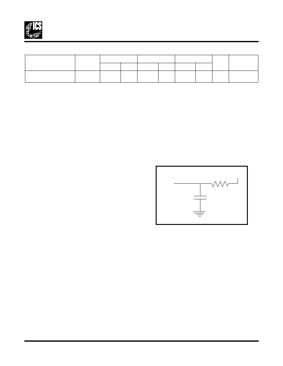
CLK
25 pF
1.4V
200
5342_03
相关PDF资料 |
PDF描述 |
|---|---|
| ICS552ARI-01LFT | 200 MHz, OTHER CLOCK GENERATOR, PDSO20 |
| ICS552R-01ILF | 200 MHz, OTHER CLOCK GENERATOR, PDSO20 |
| ICS557G-05ATR | 200 MHz, PROC SPECIFIC CLOCK GENERATOR, PDSO20 |
| ICS557G-08LF | 557 SERIES, LOW SKEW CLOCK DRIVER, 1 TRUE OUTPUT(S), 0 INVERTED OUTPUT(S), PDSO16 |
| ICS557G-08LFT | 557 SERIES, LOW SKEW CLOCK DRIVER, 1 TRUE OUTPUT(S), 0 INVERTED OUTPUT(S), PDSO16 |
相关代理商/技术参数 |
参数描述 |
|---|---|
| ICS5342-1 | 制造商:ICS 制造商全称:ICS 功能描述:Analog IC |
| ICS5342-2 | 制造商:ICS 制造商全称:ICS 功能描述:Analog IC |
| ICS5342-3 | 制造商:ICS 制造商全称:ICS 功能描述:Analog IC |
| ICS5342ADD | 制造商:ICS 制造商全称:ICS 功能描述:Addendum to ICS5342 Data Sheet |
| ICS5342V | 制造商:未知厂家 制造商全称:未知厂家 功能描述:Peripheral IC |
发布紧急采购,3分钟左右您将得到回复。