- 您现在的位置:买卖IC网 > Datasheet目录328 > IDT7026L20G (IDT, Integrated Device Technology Inc)IC SRAM 256KBIT 20NS 84PGA Datasheet资料下载
参数资料
| 型号: | IDT7026L20G |
| 厂商: | IDT, Integrated Device Technology Inc |
| 文件页数: | 15/18页 |
| 文件大小: | 0K |
| 描述: | IC SRAM 256KBIT 20NS 84PGA |
| 标准包装: | 3 |
| 格式 - 存储器: | RAM |
| 存储器类型: | SRAM - 双端口,异步 |
| 存储容量: | 256K(16K x 16) |
| 速度: | 20ns |
| 接口: | 并联 |
| 电源电压: | 4.5 V ~ 5.5 V |
| 工作温度: | 0°C ~ 70°C |
| 封装/外壳: | 84-BPGA |
| 供应商设备封装: | 84-PGA(27.94x27.94) |
| 包装: | 托盘 |
| 其它名称: | 7026L20G |
�� �
�
�IDT7026S/L�
�High-Speed� 16K� x� 16� Dual-Port� Static� RAM�
�Military,� Industrial� and� Commercial� Temperature� Ranges�
�Truth� Table� IV� —�
�Address� BUSY� Arbitration�
�Inputs� Outputs�
�A� OL� -A� 13L�
�CE� L� CE� R� A� OR� -A� 13R� BUSY� L� (1)� BUSY� R� (1)�
�Function�
�Width� Expansion� with� BUSY� Logic�
�Master/Slave� Arrays�
�When� expanding� an� IDT7026� RAM� array� in� width� while� using� BUSY�
�logic,� one� master� part� is� used� to� decide� which� side� of� the� RAM� array� will�
�receive� a� BUSY� indication,� and� to� output� that� indication.� Any� number� of�
�slaves� to� be� addressed� in� the� same� address� range� as� the� master� use� the�
�X�
�H�
�X�
�L�
�X�
�X�
�H�
�L�
�NO� MATCH�
�MATCH�
�MATCH�
�MATCH�
�H�
�H�
�H�
�(2)�
�H�
�H�
�H�
�(2)�
�Normal�
�Normal�
�Normal�
�Write� Inhibit� (3)�
�BUSY� signal� as� a� write� inhibit� signal.� Thus� on� the� IDT7026� RAM� the� BUSY�
�pin� is� an� output� if� the� part� is� used� as� a� master� (M/� S� pin� =� V� IH� ),� and� the� BUSY�
�pin� is� an� input� if� the� part� used� as� a� slave� (M/� S� pin� =� V� IL� )� as� shown� in�
�Figure� 3.�
�If� two� or� more� master� parts� were� used� when� expanding� in� width,� a� split�
�NOTES:�
�2939� tbl� 16�
�decision� could� result� with� one� master� indicating� BUSY� on� one� side� of� the�
�1.� Pins� BUSY� L� and� BUSY� R� are� both� outputs� when� the� part� is� configured� as� a�
�master.� Both� are� inputs� when� configured� as� a� slave.� BUSY� X� outputs� on� the�
�IDT7026� are� push� pull,� not� open� drain� outputs.� On� slaves� the� BUSY� X� input�
�internally� inhibits� writes.�
�2.� LOW� if� the� inputs� to� the� opposite� port� were� stable� prior� to� the� address� and� enable�
�inputs� of� this� port.� HIGH� if� the� inputs� to� the� opposite� port� became� stable� after� the�
�address� and� enable� inputs� of� this� port.� If� t� APS� is� not� met,� either� BUSY� L� or� BUSY� R�
�MASTER�
�Dual� Port�
�RAM�
�BUSY� L�
�CE�
�BUSY� R�
�SLAVE�
�Dual� Port�
�RAM�
�BUSY� L�
�CE�
�BUSY� R�
�=� LOW� will� result.� BUSY� L� and� BUSY� R� outputs� cannot� be� LOW� simultaneously.�
�3.� Writes� to� the� left� port� are� internally� ignored� when� BUSY� L� outputs� are� driving� LOW�
�regardless� of� actual� logic� level� on� the� pin.� Writes� to� the� right� port� are� internally�
�ignored� when� BUSY� R� outputs� are� driving� LOW� regardless� of� actual� logic� level�
�MASTER�
�Dual� Port�
�CE�
�SLAVE�
�Dual� Port�
�CE�
�on� the� pin.�
�BUSY� L�
�RAM�
�BUSY� L�
�BUSY� R�
�RAM�
�BUSY� L�
�BUSY� R�
�BUSY� R�
�,�
�2939� drw� 16�
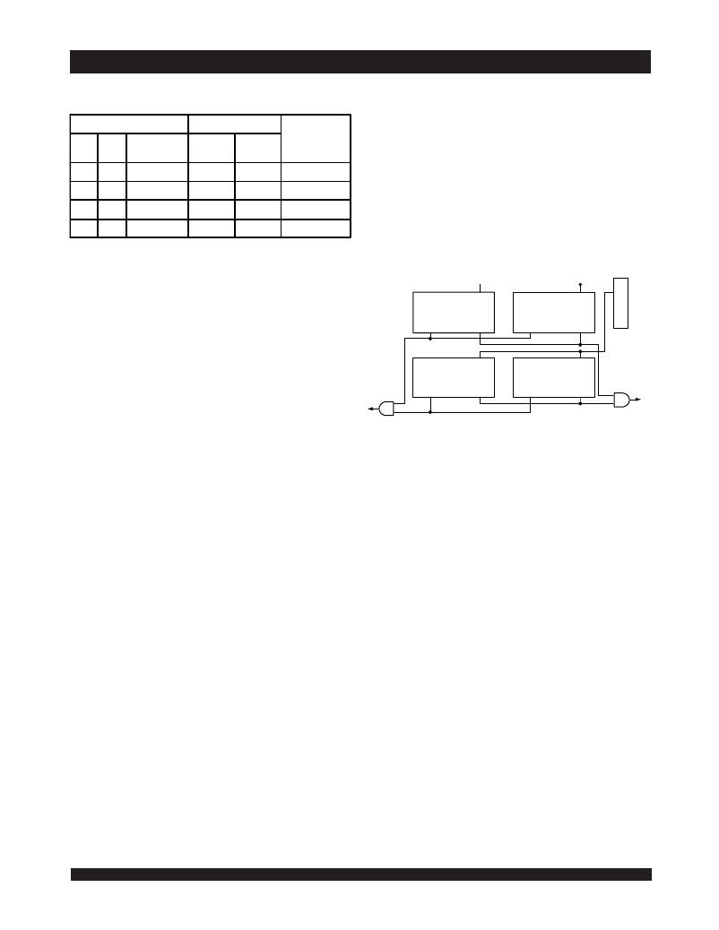
�Figure� 3.� Busy� and� chip� enable� routing� for� both� width� and� depth�
�Functional� Description�
�The� IDT7026� provides� two� ports� with� separate� control,� address� and�
�I/O� pins� that� permit� independent� access� for� reads� or� writes� to� any� location�
�in� memory.� The� IDT7026� has� an� automatic� power� down� feature� controlled�
�by� CE� .� The� CE� controls� on-chip� power� down� circuitry� that� permits� the�
�respective� port� to� go� into� a� standby� mode� when� not� selected� (� CE� =� V� IH� ).�
�When� a� port� is� enabled,� access� to� the� entire� memory� array� is� permitted.�
�Busy� Logic�
�Busy� Logic� provides� a� hardware� indication� that� both� ports� of� the� RAM�
�have� accessed� the� same� location� at� the� same� time.� It� also� allows� one� of� the�
�two� accesses� to� proceed� and� signals� the� other� side� that� the� RAM� is� “Busy”.�
�The� BUSY� pin� can� then� be� used� to� stall� the� access� until� the� operation� on�
�the� other� side� is� completed.� If� a� write� operation� has� been� attempted� from�
�the� side� that� receives� a� BUSY� indication,� the� write� signal� is� gated� internally�
�to� prevent� the� write� from� proceeding.�
�The� use� of� BUSY� logic� is� not� required� or� desirable� for� all� applications.�
�In� some� cases� it� may� be� useful� to� logically� OR� the� BUSY� outputs� together�
�and� use� any� BUSY� indication� as� an� interrupt� source� to� flag� the� event� of�
�an� illegal� or� illogical� operation.� If� the� write� inhibit� function� of� BUSY� logic� is�
�not� desirable,� the� BUSY� logic� can� be� disabled� by� placing� the� part� in� slave�
�mode� with� the� M/� S� pin.� Once� in� slave� mode� the� BUSY� pin� operates� solely�
�as� a� write� inhibit� input� pin.� Normal� operation� can� be� programmed� by� tying�
�the� BUSY� pins� HIGH.� If� desired,� unintended� write� operations� can� be�
�prevented� to� a� port� by� tying� the� BUSY� pin� for� that� port� LOW.�
�The� BUSY� outputs� on� the� IDT� 7026� RAM� in� master� mode,� are� push-�
�pull� type� outputs� and� do� not� require� pull� up� resistors� to� operate.� If� these�
�RAMs� are� being� expanded� in� depth,� then� the� BUSY� indication� for� the�
�resulting� array� requires� the� use� of� an� external� AND� gate.�
�expansion� with� IDT7026� RAMs.�
�array� and� another� master� indicating� BUSY� on� one� other� side� of� the� array.�
�This� would� inhibit� the� write� operations� from� one� port� for� part� of� a� word� and�
�inhibit� the� write� operations� from� the� other� port� for� the� other� part� of� the� word.�
�The� BUSY� arbitration� on� a� master� is� based� on� the� chip� enable� and�
�address� signals� only.� It� ignores� whether� an� access� is� a� read� or� write.� In�
�a� master/slave� array,� both� address� and� chip� enable� must� be� valid� long�
�enough� for� a� BUSY� flag� to� be� output� from� the� master� before� the� actual� write�
�pulse� can� be� initiated� with� either� the� R/� W� signal� or� the� byte� enables.� Failure�
�to� observe� this� timing� can� result� in� a� glitched� internal� write� inhibit� signal� and�
�corrupted� data� in� the� slave.�
�Semaphores�
�The� IDT7026� is� an� extremely� fast� Dual-Port� 16K� x� 16� CMOS� Static�
�RAM� with� an� additional� 8� address� locations� dedicated� to� binary� semaphore�
�flags.� These� flags� allow� either� processor� on� the� left� or� right� side� of� the� Dual-�
�Port� RAM� to� claim� a� privilege� over� the� other� processor� for� functions� defined�
�by� the� system� designer’s� software.� As� an� example,� the� semaphore� can�
�be� used� by� one� processor� to� inhibit� the� other� from� accessing� a� portion� of�
�the� Dual-Port� RAM� or� any� other� shared� resource.�
�The� Dual-Port� RAM� features� a� fast� access� time,� and� both� ports� are�
�completely� independent� of� each� other.� This� means� that� the� activity� on� the�
�left� port� in� no� way� slows� the� access� time� of� the� right� port.� Both� ports� are�
�identical� in� function� to� standard� CMOS� Static� RAM� and� can� be� read� from,�
�or� written� to,� at� the� same� time� with� the� only� possible� conflict� arising� from� the�
�simultaneous� writing� of,� or� a� simultaneous� READ/WRITE� of,� a� non-�
�semaphore� location.� Semaphores� are� protected� against� such� ambiguous�
�situations� and� may� be� used� by� the� system� program� to� avoid� any� conflicts�
�15�
�6.42�
�相关PDF资料 |
PDF描述 |
|---|---|
| IDT7027L25G | IC SRAM 512KBIT 25NS 108PGA |
| IDT7028L20PFI | IC SRAM 1MBIT 20NS 100TQFP |
| IDT7034L20PFI | IC SRAM 72KBIT 20NS 100TQFP |
| IDT7035L20PFI | IC SRAM 144KBIT 20NS 100TQFP |
| IDT7037L20PFI | IC SRAM 576KBIT 20NS 100TQFP |
相关代理商/技术参数 |
参数描述 |
|---|---|
| IDT7026L20J | 功能描述:IC SRAM 256KBIT 20NS 84PLCC RoHS:否 类别:集成电路 (IC) >> 存储器 系列:- 标准包装:1,000 系列:- 格式 - 存储器:RAM 存储器类型:SRAM - 双端口,同步 存储容量:1.125M(32K x 36) 速度:5ns 接口:并联 电源电压:3.15 V ~ 3.45 V 工作温度:-40°C ~ 85°C 封装/外壳:256-LBGA 供应商设备封装:256-CABGA(17x17) 包装:带卷 (TR) 其它名称:70V3579S5BCI8 |
| IDT7026L20J8 | 功能描述:IC SRAM 256KBIT 20NS 84PLCC RoHS:否 类别:集成电路 (IC) >> 存储器 系列:- 标准包装:1,000 系列:- 格式 - 存储器:RAM 存储器类型:SRAM - 双端口,同步 存储容量:1.125M(32K x 36) 速度:5ns 接口:并联 电源电压:3.15 V ~ 3.45 V 工作温度:-40°C ~ 85°C 封装/外壳:256-LBGA 供应商设备封装:256-CABGA(17x17) 包装:带卷 (TR) 其它名称:70V3579S5BCI8 |
| IDT7026L20JI | 功能描述:IC SRAM 256KBIT 20NS 84PLCC RoHS:否 类别:集成电路 (IC) >> 存储器 系列:- 标准包装:1,000 系列:- 格式 - 存储器:RAM 存储器类型:SRAM - 双端口,同步 存储容量:1.125M(32K x 36) 速度:5ns 接口:并联 电源电压:3.15 V ~ 3.45 V 工作温度:-40°C ~ 85°C 封装/外壳:256-LBGA 供应商设备封装:256-CABGA(17x17) 包装:带卷 (TR) 其它名称:70V3579S5BCI8 |
| IDT7026L20JI8 | 功能描述:IC SRAM 256KBIT 20NS 84PLCC RoHS:否 类别:集成电路 (IC) >> 存储器 系列:- 标准包装:1,000 系列:- 格式 - 存储器:RAM 存储器类型:SRAM - 双端口,同步 存储容量:1.125M(32K x 36) 速度:5ns 接口:并联 电源电压:3.15 V ~ 3.45 V 工作温度:-40°C ~ 85°C 封装/外壳:256-LBGA 供应商设备封装:256-CABGA(17x17) 包装:带卷 (TR) 其它名称:70V3579S5BCI8 |
| IDT7026L25G | 功能描述:IC SRAM 256KBIT 25NS 84PGA RoHS:否 类别:集成电路 (IC) >> 存储器 系列:- 标准包装:3,000 系列:- 格式 - 存储器:EEPROMs - 串行 存储器类型:EEPROM 存储容量:8K (1K x 8) 速度:400kHz 接口:I²C,2 线串口 电源电压:1.7 V ~ 5.5 V 工作温度:-40°C ~ 85°C 封装/外壳:8-SOIC(0.154",3.90mm 宽) 供应商设备封装:8-SOIC 包装:带卷 (TR) |
发布紧急采购,3分钟左右您将得到回复。