参数资料
| 型号: | ISL6323BCRZ |
| 厂商: | Intersil |
| 文件页数: | 27/36页 |
| 文件大小: | 0K |
| 描述: | IC PWM CTRLR SYNC BUCK DL 48QFN |
| 标准包装: | 43 |
| 应用: | 控制器,AMD SVI |
| 输入电压: | 5 V ~ 12 V |
| 输出数: | 2 |
| 输出电压: | 最高 2V |
| 工作温度: | 0°C ~ 70°C |
| 安装类型: | 表面贴装 |
| 封装/外壳: | 48-VFQFN 裸露焊盘 |
| 供应商设备封装: | 48-QFN(7x7) |
| 包装: | 管件 |
第1页第2页第3页第4页第5页第6页第7页第8页第9页第10页第11页第12页第13页第14页第15页第16页第17页第18页第19页第20页第21页第22页第23页第24页第25页第26页当前第27页第28页第29页第30页第31页第32页第33页第34页第35页第36页
�� �
�
�ISL6323B�
�1.6�
�1.4�
�1.2�
�1.0�
�0.8�
�0.6�
�Q� GATE� = 100nC�
�In� Equations� 28� and� 29,� P� Qg_Q1� is� the� total� upper� gate� drive�
�power� loss� and� P� Qg_Q2� is� the� total� lower� gate� drive� power�
�loss;� the� gate� charge� (Q� G1� and� Q� G2� )� is� defined� at� the�
�particular� gate� to� source� drive� voltage� PVCC� in� the�
�corresponding� MOSFET� data� sheet;� I� Q� is� the� driver� total�
�quiescent� current� with� no� load� at� both� drive� outputs;� N� Q1� and�
�N� Q2� are� the� number� of� upper� and� lower� MOSFETs� per� phase,�
�respectively;� N� PHASE� is� the� number� of� active� phases.� The�
�I� Q*� VCC� product� is� the� quiescent� power� of� the� controller�
�without� capacitive� load� and� is� typically� 75mW� at� 300kHz.�
�0.4�
�0.2�
�20nC�
�50nC�
�PVCC�
�BOOT�
�C� GD�
�D�
�0.0�
�0.0�
�0.1�
�0.2�
�0.3�
�0.4�
�0.5�
�0.6�
�0.7�
�0.8�
�0.9�
�1.0�
�R� HI1�
�UGATE�
�G�
�C� DS�
�Δ� V� BOOT_CAP� (V)�
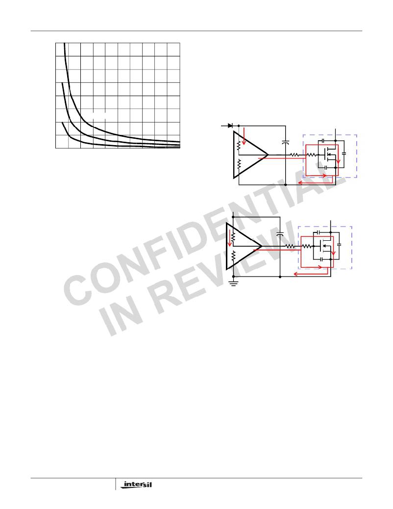
�FIGURE� 17.� BOOTSTRAP� CAPACITANCE� vs� BOOT� RIPPLE�
�VOLTAGE�
�R� LO1�
�R� G1�
�R� GI1�
�C� GS�
�Q1�
�Package� Power� Dissipation�
�When� choosing� MOSFETs� it� is� important� to� consider� the�
�amount� of� power� being� dissipated� in� the� integrated� drivers�
�located� in� the� controller.� Since� there� are� a� total� of� three�
�drivers� in� the� controller� package,� the� total� power� dissipated�
�by� all� three� drivers� must� be� less� than� the� maximum�
�allowable� power� dissipation� for� the� QFN� package.�
�S�
�PHASE�
�FIGURE� 18.� TYPICAL� UPPER-GATE� DRIVE� TURN-ON� PATH�
�PVCC�
�D�
�C� GD�
�Calculating� the� power� dissipation� in� the� drivers� for� a� desired�
�application� is� critical� to� ensure� safe� operation.� Exceeding� the�
�maximum� allowable� power� dissipation� level� will� push� the� IC�
�beyond� the� maximum� recommended� operating� junction�
�R� HI2�
�R� LO2�
�LGATE�
�G�
�R� G2�
�R� GI2�
�C� GS�
�C� DS�
�Q2�
�temperature� of� +125°C.� The� maximum� allowable� IC� power�
�dissipation� for� the� 7x7� QFN� package� is� approximately� 3.5W�
��S�
�FIGURE� 19.� TYPICAL� LOWER-GATE� DRIVE� TURN-ON� PATH�
��The� total� gate� drive� power� losses� are� dissipated� among� the�
�When� designing� the� ISL6323B� into� an� application,� it� is�
�recommended� that� the� following� calculation� is� used� to�
�ensure� safe� operation� at� the� desired� frequency� for� the�
�selected� MOSFETs.� The� total� gate� drive� power� losses,�
�P� Qg_TOT� ,� due� to� the� gate� charge� of� MOSFETs� and� the�
�integrated� driver� ’s� internal� circuitry� and� their� corresponding�
�average� driver� current� can� be� estimated� with� Equations� 28�
�and� 29,� respectively.�
�resistive� components� along� the� transition� path� and� in� the�
�bootstrap� diode.� The� portion� of� the� total� power� dissipated� in�
�the� controller� itself� is� the� power� dissipated� in� the� upper� drive�
�path� resistance� (P� DR_UP� ),� the� lower� drive� path� resistance�
�(P� DR_UP� ),� and� in� the� boot� strap� diode� (P� BOOT� ).� The� rest� of�
�the� power� will� be� dissipated� by� the� external� gate� resistors�
�(R� G1� and� R� G2� )� and� the� internal� gate� resistors� (R� GI1� and�
�R� GI2� )� of� the� MOSFETs.� Figures� 18� and� 19� show� the� typical�
�P� Qg_Q1� =� ---� ?� Q� G1� ?� PVCC� ?� F� SW� ?� N� Q1� ?� N� PHASE�
�P� Qg_TOT� =� P� Qg_Q1� +� P� Qg_Q2� +� I� Q� ?� VCC�
�3�
�2�
�P� Qg_Q2� =� Q� G2� ?� PVCC� ?� F� SW� ?� N� Q2� ?� N� PHASE�
�(EQ.� 28)�
�upper� and� lower� gate� drives� turn-on� transition� path.� The� total�
�power� dissipation� in� the� controller� itself,� P� DR� ,� can� be� roughly�
�estimated� as� Equation� 30:�
�Inductor� DCR� Current� Sensing� Component�
�Selection� and� R� SET� Value� Calculation�
�I� DR� =� ?� ---� ?� Q� G1� ?� N�
�3�
�?� 2�
�Q1�
�?�
�+� Q� G2� ?� N� Q2� ?� ?� N� PHASE� ?� F� SW� +� I� Q�
�(EQ.� 29)�
�With� the� single� R� SET� resistor� setting� the� value� of� the�
�effective� internal� sense� resistors� for� both� the� North� Bridge�
�and� Core� regulators,� it� is� important� to� set� the� R� SET� value�
�and� the� inductor� RC� filter� gain,� K,� properly.� See� “Continuous�
�Current� Sampling”� on� page� 14� and� “Channel-Current�
�Balance”� on� page� 15� for� more� details� on� the� application� of�
�the� R� SET� resistor� and� the� RC� filter� gain.�
�27�
�FN6879.1�
�May� 12,� 2010�
�相关PDF资料 |
PDF描述 |
|---|---|
| RCA18DTMT | CONN EDGECARD 36POS R/A .125 SLD |
| ISL6323ACRZ | IC PWM CTRLR SYNC BUCK DL 48QFN |
| LD6806CX4/25H,315 | IC REG LDO 2.5V .2A 4WLCSP |
| 420USC390MEFCSN30X40 | CAP ALUM 390UF 420V 20% SNAP-IN |
| 2256-19L | POWER CHOKE 33UH MOLDED AXIAL |
相关代理商/技术参数 |
参数描述 |
|---|---|
| ISL6323BCRZR5381 | 制造商:Intersil Corporation 功能描述:4+1 PHASE CONT. FOR CORE+NORTHBRIDGE, 2 PHASE PSI, 3.4MHZ SV - Rail/Tube 制造商:Intersil Corporation 功能描述:IC PWM CTRLR SYNC BUCK DL 48QFN 制造商:Intersil 功能描述:4+1 PHS CONT CORE + NORTHBRDG PROG |
| ISL6323BCRZ-T | 功能描述:IC PWM CTRLR SYNC BUCK DL 48QFN RoHS:是 类别:集成电路 (IC) >> PMIC - 稳压器 - 专用型 系列:- 标准包装:43 系列:- 应用:控制器,Intel VR11 输入电压:5 V ~ 12 V 输出数:1 输出电压:0.5 V ~ 1.6 V 工作温度:-40°C ~ 85°C 安装类型:表面贴装 封装/外壳:48-VFQFN 裸露焊盘 供应商设备封装:48-QFN(7x7) 包装:管件 |
| ISL6323BCRZ-TR5381 | 制造商:Intersil Corporation 功能描述:4+1 PHASE CONT. FOR CORE+NORTHBRIDGE, 2 PHASE PSI, 3.4MHZ S - Tape and Reel 制造商:Intersil Corporation 功能描述:IC PWM CTRLR SYNC BUCK DL 48QFN 制造商:Intersil 功能描述:4+1 PHS CONT CORE + NORTHBRDG PROG |
| ISL6323BCRZ-TR5453 | 制造商:Intersil Corporation 功能描述:STD. ISL6323BCRZ-T WITH GOLD BOND WIRE ONLY, T&R - Tape and Reel |
| ISL6323BIRZ | 功能描述:IC PWM CTRLR SYNC BUCK DL 48QFN RoHS:是 类别:集成电路 (IC) >> PMIC - 稳压器 - 专用型 系列:- 标准包装:43 系列:- 应用:控制器,Intel VR11 输入电压:5 V ~ 12 V 输出数:1 输出电压:0.5 V ~ 1.6 V 工作温度:-40°C ~ 85°C 安装类型:表面贴装 封装/外壳:48-VFQFN 裸露焊盘 供应商设备封装:48-QFN(7x7) 包装:管件 |
发布紧急采购,3分钟左右您将得到回复。