参数资料
| 型号: | ISL6545IBZ-T |
| 厂商: | Intersil |
| 文件页数: | 10/16页 |
| 文件大小: | 0K |
| 描述: | IC REG CTRLR BUCK PWM VM 8-SOIC |
| 标准包装: | 1 |
| PWM 型: | 电压模式 |
| 输出数: | 1 |
| 频率 - 最大: | 330kHz |
| 占空比: | 100% |
| 电源电压: | 4.5 V ~ 14.4 V |
| 降压: | 是 |
| 升压: | 无 |
| 回扫: | 无 |
| 反相: | 无 |
| 倍增器: | 无 |
| 除法器: | 无 |
| Cuk: | 无 |
| 隔离: | 无 |
| 工作温度: | -40°C ~ 85°C |
| 封装/外壳: | 8-SOIC(0.154",3.90mm 宽) |
| 包装: | 标准包装 |
| 产品目录页面: | 1243 (CN2011-ZH PDF) |
| 其它名称: | ISL6545IBZ-TDKR |
�� �
�
�ISL6545,� ISL6545A�
�sense� resistor),� the� regular� boot� refresh� circuit� will� still� be�
�active.�
�Current� Sinking�
�The� ISL6545x� incorporates� a� MOSFET� shoot-through�
�protection� method� which� allows� a� converter� to� sink� current�
�capacitors� C� IN� and� C� O� may� each� represent� numerous� physical�
�capacitors.� For� best� results,� locate� the� ISL6545x� within� 1� inch�
�of� the� MOSFETs,� Q� 1� and� Q� 2� .� The� circuit� traces� for� the�
�MOSFET� gate� and� source� connections� from� the� ISL6545x�
�must� be� sized� to� handle� up� to� 1A� peak� current.�
�as� well� as� source� current.� Care� should� be� exercised� when�
�designing� a� converter� with� the� ISL6545x� when� it� is� known�
�that� the� converter� may� sink� current.�
�When� the� converter� is� sinking� current,� it� is� behaving� as� a�
�ISL6545,�
�BOOT�
�C� BOOT�
�PHASE�
�+V� IN�
�Q� 1�
�L� O�
�V� OUT�
�boost� converter� that� is� regulating� its� input� voltage.� This�
�means� that� the� converter� is� boosting� current� into� the� V� CC�
�ISL6545A�
�LGATE/OCSET�
�VCC�
�+V� CC�
�Q� 2�
�C� O�
�rail,� which� supplies� the� bias� voltage� to� the� ISL6545x.� If� there�
�is� nowhere� for� this� current� to� go,� such� as� to� other� distributed�
�loads� on� the� V� CC� rail,� through� a� voltage� limiting� protection�
�device,� or� other� methods,� the� capacitance� on� the� V� CC� bus�
�will� absorb� the� current.� This� situation� will� allow� voltage� level�
�of� the� V� CC� rail� to� increase.� If� the� voltage� level� of� the� rail� is�
�boosted� to� a� level� that� exceeds� the� maximum� voltage� rating�
�of� the� ISL6545x,� then� the� IC� will� experience� an� irreversible�
�failure� and� the� converter� will� no� longer� be� operational.�
�Ensuring� that� there� is� a� path� for� the� current� to� follow� other�
�than� the� capacitance� on� the� rail� will� prevent� this� failure�
�mode.�
�Application� Guidelines�
�Layout� Considerations�
�As� in� any� high� frequency� switching� converter,� layout� is� very�
�important.� Switching� current� from� one� power� device� to� another�
�can� generate� voltage� transients� across� the� impedances� of� the�
�interconnecting� bond� wires� and� circuit� traces.� These�
�interconnecting� impedances� should� be� minimized� by� using�
�wide,� short� printed� circuit� traces.� The� critical� components�
�should� be� located� as� close� together� as� possible,� using� ground�
�plane� construction� or� single� point� grounding.�
�V� IN�
�ISL6545,�
�ISL6545A�
�C� VCC�
�GND�
�FIGURE� 8.� PRINTED� CIRCUIT� BOARD� SMALL� SIGNAL�
�LAYOUT� GUIDELINES�
�Figure� 8� shows� the� circuit� traces� that� require� additional�
�layout� consideration.� Use� single� point� and� ground� plane�
�construction� for� the� circuits� shown.� Minimize� any� leakage�
�current� paths� on� the� COMP/SD� pin� and� locate� the� resistor,�
�R� OSCET� close� to� the� COMP/SD� pin� because� the� internal�
�current� source� is� only� 20μA.� Provide� local� V� CC� decoupling�
�between� V� CC� and� GND� pins.� Locate� the� capacitor,� C� BOOT�
�as� close� as� practical� to� the� BOOT� and� PHASE� pins.� All�
�components� used� for� feedback� compensation� (not� shown)�
�should� be� located� as� close� to� the� IC� as� practical.�
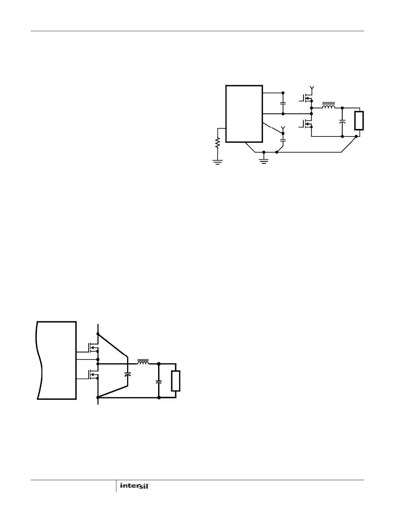
�Feedback� Compensation�
�This� section� highlights� the� design� consideration� for� a�
�voltage-mode� controller� requiring� external� compensation.� To�
�address� a� broad� range� of� applications,� a� type-3� feedback�
�network� is� recommended,� as� shown� in� the� top� part� of�
�Figure� 9.�
�Figure� 9� also� highlights� the� voltage-mode� control� loop� for� a�
�synchronous-rectified� buck� converter,� applicable� to� the�
�ISL6545x� circuit.� The� output� voltage� (V� OUT� )� is� regulated� to� the�
�UGATE�
�PHASE�
�Q� 1�
�L� O�
�V� OUT�
�reference� voltage,� V� REF� .� The� error� amplifier� output� (COMP� pin�
�voltage)� is� compared� with� the� oscillator� (OSC)� modified�
�sawtooth� wave� to� provide� a� pulse-width� modulated� wave� with�
�LGATE/OCSET�
�Q� 2�
�C� IN�
�C� O�
�an� amplitude� of� V� IN� at� the� PHASE� node.� The� PWM� wave� is�
�smoothed� by� the� output� filter� (L� and� C).� The� output� filter�
�capacitor� bank’s� equivalent� series� resistance� is� represented� by�
�the� series� resistor� E.�
�RETURN�
�FIGURE� 7.� PRINTED� CIRCUIT� BOARD� POWER� AND�
�GROUND� PLANES� OR� ISLANDS�
�Figure� 7� shows� the� critical� power� components� of� the� converter.�
�To� minimize� the� voltage� overshoot,� the� interconnecting� wires�
�indicated� by� heavy� lines� should� be� part� of� a� ground� or� power�
�plane� in� a� printed� circuit� board.� The� components� shown� should�
�be� located� as� close� together� as� possible.� Please� note� that� the�
�10�
�FN6305.6�
�March� 3,� 2011�
�相关PDF资料 |
PDF描述 |
|---|---|
| ISL6548ACRZA-T | IC REG/CTLR ACPI DUAL DDR 28QFN |
| ISL6548CRZA | IC REG/CTRLR ACPI DUAL DDR 28QFN |
| ISL6551IR-T | IC REG CTRLR FLYBACK PWM 28-QFN |
| ISL6552CR-T | IC REG CTRLR BUCK PWM 20-QFN |
| ISL6553CB-T | IC REG CTRLR BUCK PWM 16-SOIC |
相关代理商/技术参数 |
参数描述 |
|---|---|
| ISL6545IRZ | 功能描述:IC REG CTRLR BUCK PWM VM 10-DFN RoHS:是 类别:集成电路 (IC) >> PMIC - 稳压器 - DC DC 切换控制器 系列:- 产品培训模块:Lead (SnPb) Finish for COTS Obsolescence Mitigation Program 标准包装:2,500 系列:- PWM 型:电流模式 输出数:1 频率 - 最大:275kHz 占空比:50% 电源电压:18 V ~ 110 V 降压:无 升压:无 回扫:无 反相:无 倍增器:无 除法器:无 Cuk:无 隔离:是 工作温度:-40°C ~ 85°C 封装/外壳:8-SOIC(0.154",3.90mm 宽) 包装:带卷 (TR) |
| ISL6545IRZ-T | 功能描述:IC REG CTRLR BUCK PWM VM 10-DFN RoHS:是 类别:集成电路 (IC) >> PMIC - 稳压器 - DC DC 切换控制器 系列:- 产品培训模块:Lead (SnPb) Finish for COTS Obsolescence Mitigation Program 标准包装:2,500 系列:- PWM 型:电流模式 输出数:1 频率 - 最大:275kHz 占空比:50% 电源电压:18 V ~ 110 V 降压:无 升压:无 回扫:无 反相:无 倍增器:无 除法器:无 Cuk:无 隔离:是 工作温度:-40°C ~ 85°C 封装/外壳:8-SOIC(0.154",3.90mm 宽) 包装:带卷 (TR) |
| ISL6546IRZ | 功能描述:IC REG BUCK SYNC 1.2A 10-QFN RoHS:是 类别:集成电路 (IC) >> PMIC - 稳压器 - DC DC 开关稳压器 系列:- 产品培训模块:Lead (SnPb) Finish for COTS Obsolescence Mitigation Program 标准包装:1 系列:- 类型:降压(降压) 输出类型:固定 输出数:1 输出电压:3.3V 输入电压:4.5 V ~ 24 V PWM 型:- 频率 - 开关:- 电流 - 输出:125mA 同步整流器:无 工作温度:-40°C ~ 85°C 安装类型:表面贴装 封装/外壳:SOT-23-6 包装:Digi-Reel® 供应商设备封装:SOT-6 其它名称:MAX1836EUT33#TG16DKR |
| ISL6546IRZ-T | 功能描述:IC REG BUCK SYNC 1.2A 10-QFN RoHS:是 类别:集成电路 (IC) >> PMIC - 稳压器 - DC DC 开关稳压器 系列:- 产品培训模块:Lead (SnPb) Finish for COTS Obsolescence Mitigation Program 标准包装:1 系列:- 类型:降压(降压) 输出类型:固定 输出数:1 输出电压:3.3V 输入电压:4.5 V ~ 24 V PWM 型:- 频率 - 开关:- 电流 - 输出:125mA 同步整流器:无 工作温度:-40°C ~ 85°C 安装类型:表面贴装 封装/外壳:SOT-23-6 包装:Digi-Reel® 供应商设备封装:SOT-6 其它名称:MAX1836EUT33#TG16DKR |
| ISL6548A-6506EVAL1Z | 功能描述:EVALUATION BOARD ISL6548A-6506 RoHS:是 类别:编程器,开发系统 >> 评估板 - DC/DC 与 AC/DC(离线)SMPS 系列:- 产品培训模块:Obsolescence Mitigation Program 标准包装:1 系列:True Shutdown™ 主要目的:DC/DC,步升 输出及类型:1,非隔离 功率 - 输出:- 输出电压:- 电流 - 输出:1A 输入电压:2.5 V ~ 5.5 V 稳压器拓扑结构:升压 频率 - 开关:3MHz 板类型:完全填充 已供物品:板 已用 IC / 零件:MAX8969 |
发布紧急采购,3分钟左右您将得到回复。