参数资料
| 型号: | ISL6545IBZ-T |
| 厂商: | Intersil |
| 文件页数: | 11/16页 |
| 文件大小: | 0K |
| 描述: | IC REG CTRLR BUCK PWM VM 8-SOIC |
| 标准包装: | 1 |
| PWM 型: | 电压模式 |
| 输出数: | 1 |
| 频率 - 最大: | 330kHz |
| 占空比: | 100% |
| 电源电压: | 4.5 V ~ 14.4 V |
| 降压: | 是 |
| 升压: | 无 |
| 回扫: | 无 |
| 反相: | 无 |
| 倍增器: | 无 |
| 除法器: | 无 |
| Cuk: | 无 |
| 隔离: | 无 |
| 工作温度: | -40°C ~ 85°C |
| 封装/外壳: | 8-SOIC(0.154",3.90mm 宽) |
| 包装: | 标准包装 |
| 产品目录页面: | 1243 (CN2011-ZH PDF) |
| 其它名称: | ISL6545IBZ-TDKR |
�� �
�
�ISL6545,� ISL6545A�
�V� OSC� ?� R1� ?� F� 0�
�d� MAX� ?� V� IN� ?� F� LC�
�C2�
�R2� =� ---------------------------------------------�
�(EQ.� 4)�
�COMP�
�R2�
�C1�
�R3�
�C3�
�2.� Calculate� C1� such� that� F� Z1� is� placed� at� a� fraction� of� the� F� LC� ,�
�at� 0.1� to� 0.75� of� F� LC� (to� adjust,� change� the� 0.5� factor� to�
�-�
�desired� number).� The� higher� the� quality� factor� of� the� output�
�E/A�
�+�
�FB�
�Ro�
�R1�
�filter� and/or� the� higher� the� ratio� F� CE� /F� LC� ,� the� lower� the� F� Z1�
�frequency� (to� maximize� phase� boost� at� F� LC� ).�
�C1� =� ------------------------------------------------�
�VREF�
�1�
�2� π� ?� R2� ?� 0.5� ?� F� LC�
�(EQ.� 5)�
�C2� =� ---------------------------------------------------------�
�PWM�
�OSCILLATOR�
�V� OSC�
�V� IN�
�V� OUT�
�3.� Calculate� C2� such� that� F� P1� is� placed� at� F� CE� .�
�C1�
�2� π� ?� R2� ?� C1� ?� F� CE� –� 1�
�(EQ.� 6)�
�CIRCUIT�
�UGATE�
�L�
�D�
�4.� Calculate� R3� such� that� F� Z2� is� placed� at� F� LC� .� Calculate� C3�
�such� that� F� P2� is� placed� below� F� SW� (typically,� 0.5� to� 1.0�
�HALF-BRIDGE�
�times� F� SW� ).� F� SW� represents� the� switching� frequency.�
�DRIVE�
�PHASE�
�LGATE�
�C�
�E�
�Change� the� numerical� factor� to� reflect� desired� placement�
�of� this� pole.� Placement� of� F� P2� lower� in� frequency� helps�
�reduce� the� gain� of� the� compensation� network� at� high�
�frequency,� in� turn� reducing� the� HF� ripple� component� at�
�the� COMP� pin� and� minimizing� resultant� duty� cycle� jitter.�
�R3� =� ----------------------�
�F� SW�
�C3� =� -------------------------------------------------�
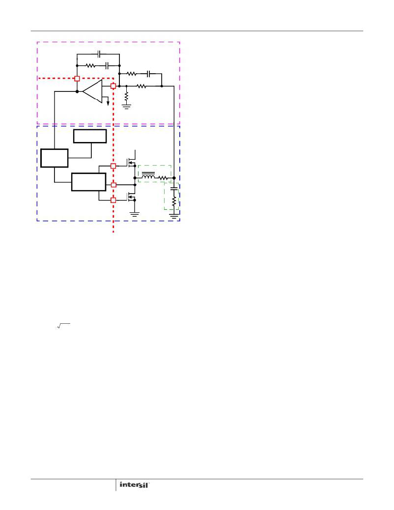
�ISL6545x� EXTERNAL� CIRCUIT�
�FIGURE� 9.� VOLTAGE-MODE� BUCK� CONVERTER�
�R1�
�------------� –� 1�
�F� LC�
�1�
�2� π� ?� R3� ?� 0.7� ?� F� SW�
�(EQ.� 7)�
�COMPENSATION� DESIGN�
�It� is� recommended� a� mathematical� model� is� used� to� plot� the�
�F� LC� =� ---------------------------�
�F� CE� =� ------------------------�
�d� MAX� ?� V� IN� 1� +� s� (� f� )� ?� E� ?� C�
�G� MOD� (� f� )� =� ------------------------------� ?� ----------------------------------------------------------------------------------------�
�V� OSC�
�1� +� s� (� f� )� ?� (� E� +� D� )� ?� C� +� s� (� f� )� ?� L� ?� C�
�The� modulator� transfer� function� is� the� small-signal� transfer�
�function� of� V� OUT� /V� COMP� .� This� function� is� dominated� by� a� DC�
�gain,� given� by� d� MAX� V� IN� /V� OSC� ,� and� shaped� by� the� output�
�filter,� with� a� double� pole� break� frequency� at� F� LC� and� a� zero� at�
�F� CE� .� For� the� purpose� of� this� analysis,� L� and� D� represent� the�
�channel� inductance� and� its� DCR,� while� C� and� E� represent� the�
�total� output� capacitance� and� its� equivalent� series� resistance.�
�1� 1�
�2� π� ?� L� ?� C� 2� π� ?� C� ?� E� (EQ.� 3)�
�loop� response.� Check� the� loop� gain� against� the� error�
�amplifier� ’s� open-loop� gain.� Verify� phase� margin� results� and�
�adjust� as� necessary.� The� equations� shown� in� Equations� 8�
�and� 9� describe� the� frequency� response� of� the� modulator�
�(G� MOD� ),� feedback� compensation� (G� FB� )� and� closed-loop�
�response� (G� CL� ):�
�2�
�G� FB� (� f� )� =� ------------------------------------------------------� ?�
�?� -----------------------------------------------------------------------------------------------------------------------------�
�(� 1� +� s� (� f� )� ?� R3� ?� C3� )� ?� ?� 1� +� s� (� f� )� ?� R2� ?� ?� ----------------------� ?� ?�
�The� compensation� network� consists� of� the� error� amplifier�
�(internal� to� the� ISL6545x)� and� the� external� R1-R3,� C1-C3�
�components.� The� goal� of� the� compensation� network� is� to�
�provide� a� closed� loop� transfer� function� with� high� 0dB� crossing�
�1� +� s� (� f� )� ?� R2� ?� C1�
�s� (� f� )� ?� R1� ?� (� C1� +� C2� )�
�1� +� s� (� f� )� ?� (� R1� +� R3� )� ?� C3�
�C1� ?� C2�
�?� ?� C1� +� C2� ?� ?�
�(EQ.� 8)�
�frequency� (F� 0� ;� typically� 0.1� to� 0.3� of� F� SW� )� and� adequate� phase�
�margin� (better� than� 45°).� Phase� margin� is� the� difference�
�between� the� closed� loop� phase� at� F� 0dB� and� 180°.� The�
�G� CL� (� f� )� =� G� MOD� (� f� )� ?� G� FB� (� f� )�
�where� ,� s� (� f� )� =� 2� π� ?� f� ?� j�
�equations� that� follow� relate� the� compensation� network’s� poles,�
�COMPENSATION� BREAK� FREQUENCY� EQUATIONS�
�F� Z1� =� --------------------------------�
�F� P1� =� -----------------------------------------------�
�2� π� ?� R2� ?� ----------------------�
�F� Z2� =� ---------------------------------------------------�
�F� P2� =� --------------------------------�
�zeros� and� gain� to� the� components� (R1,� R2,� R3,� C1,� C2,� and�
�C3)� in� Figure� 9.� Use� the� following� guidelines� for� locating� the�
�poles� and� zeros� of� the� compensation� network:�
�1.� Select� a� value� for� R1� (1k� Ω� to� 5k� Ω� ,� typically).� Calculate�
�value� for� R2� for� desired� converter� bandwidth� (F� 0� ).� If�
�1�
�2� π� ?� R2� ?� C1�
�1�
�2� π� ?� (� R1� +� R3� )� ?� C3�
�1�
�C1� ?� C2�
�C1� +� C2�
�1�
�2� π� ?� R3� ?� C3�
�(EQ.� 9)�
�setting� the� output� voltage� via� an� offset� resistor� connected�
�to� the� FB� pin,� Ro� in� Figure� 9,� the� design� procedure� can�
�be� followed� as� presented.�
�11�
�FN6305.6�
�March� 3,� 2011�
�相关PDF资料 |
PDF描述 |
|---|---|
| ISL6548ACRZA-T | IC REG/CTLR ACPI DUAL DDR 28QFN |
| ISL6548CRZA | IC REG/CTRLR ACPI DUAL DDR 28QFN |
| ISL6551IR-T | IC REG CTRLR FLYBACK PWM 28-QFN |
| ISL6552CR-T | IC REG CTRLR BUCK PWM 20-QFN |
| ISL6553CB-T | IC REG CTRLR BUCK PWM 16-SOIC |
相关代理商/技术参数 |
参数描述 |
|---|---|
| ISL6545IRZ | 功能描述:IC REG CTRLR BUCK PWM VM 10-DFN RoHS:是 类别:集成电路 (IC) >> PMIC - 稳压器 - DC DC 切换控制器 系列:- 产品培训模块:Lead (SnPb) Finish for COTS Obsolescence Mitigation Program 标准包装:2,500 系列:- PWM 型:电流模式 输出数:1 频率 - 最大:275kHz 占空比:50% 电源电压:18 V ~ 110 V 降压:无 升压:无 回扫:无 反相:无 倍增器:无 除法器:无 Cuk:无 隔离:是 工作温度:-40°C ~ 85°C 封装/外壳:8-SOIC(0.154",3.90mm 宽) 包装:带卷 (TR) |
| ISL6545IRZ-T | 功能描述:IC REG CTRLR BUCK PWM VM 10-DFN RoHS:是 类别:集成电路 (IC) >> PMIC - 稳压器 - DC DC 切换控制器 系列:- 产品培训模块:Lead (SnPb) Finish for COTS Obsolescence Mitigation Program 标准包装:2,500 系列:- PWM 型:电流模式 输出数:1 频率 - 最大:275kHz 占空比:50% 电源电压:18 V ~ 110 V 降压:无 升压:无 回扫:无 反相:无 倍增器:无 除法器:无 Cuk:无 隔离:是 工作温度:-40°C ~ 85°C 封装/外壳:8-SOIC(0.154",3.90mm 宽) 包装:带卷 (TR) |
| ISL6546IRZ | 功能描述:IC REG BUCK SYNC 1.2A 10-QFN RoHS:是 类别:集成电路 (IC) >> PMIC - 稳压器 - DC DC 开关稳压器 系列:- 产品培训模块:Lead (SnPb) Finish for COTS Obsolescence Mitigation Program 标准包装:1 系列:- 类型:降压(降压) 输出类型:固定 输出数:1 输出电压:3.3V 输入电压:4.5 V ~ 24 V PWM 型:- 频率 - 开关:- 电流 - 输出:125mA 同步整流器:无 工作温度:-40°C ~ 85°C 安装类型:表面贴装 封装/外壳:SOT-23-6 包装:Digi-Reel® 供应商设备封装:SOT-6 其它名称:MAX1836EUT33#TG16DKR |
| ISL6546IRZ-T | 功能描述:IC REG BUCK SYNC 1.2A 10-QFN RoHS:是 类别:集成电路 (IC) >> PMIC - 稳压器 - DC DC 开关稳压器 系列:- 产品培训模块:Lead (SnPb) Finish for COTS Obsolescence Mitigation Program 标准包装:1 系列:- 类型:降压(降压) 输出类型:固定 输出数:1 输出电压:3.3V 输入电压:4.5 V ~ 24 V PWM 型:- 频率 - 开关:- 电流 - 输出:125mA 同步整流器:无 工作温度:-40°C ~ 85°C 安装类型:表面贴装 封装/外壳:SOT-23-6 包装:Digi-Reel® 供应商设备封装:SOT-6 其它名称:MAX1836EUT33#TG16DKR |
| ISL6548A-6506EVAL1Z | 功能描述:EVALUATION BOARD ISL6548A-6506 RoHS:是 类别:编程器,开发系统 >> 评估板 - DC/DC 与 AC/DC(离线)SMPS 系列:- 产品培训模块:Obsolescence Mitigation Program 标准包装:1 系列:True Shutdown™ 主要目的:DC/DC,步升 输出及类型:1,非隔离 功率 - 输出:- 输出电压:- 电流 - 输出:1A 输入电压:2.5 V ~ 5.5 V 稳压器拓扑结构:升压 频率 - 开关:3MHz 板类型:完全填充 已供物品:板 已用 IC / 零件:MAX8969 |
发布紧急采购,3分钟左右您将得到回复。