参数资料
| 型号: | ISL6545IBZ-T |
| 厂商: | Intersil |
| 文件页数: | 9/16页 |
| 文件大小: | 0K |
| 描述: | IC REG CTRLR BUCK PWM VM 8-SOIC |
| 标准包装: | 1 |
| PWM 型: | 电压模式 |
| 输出数: | 1 |
| 频率 - 最大: | 330kHz |
| 占空比: | 100% |
| 电源电压: | 4.5 V ~ 14.4 V |
| 降压: | 是 |
| 升压: | 无 |
| 回扫: | 无 |
| 反相: | 无 |
| 倍增器: | 无 |
| 除法器: | 无 |
| Cuk: | 无 |
| 隔离: | 无 |
| 工作温度: | -40°C ~ 85°C |
| 封装/外壳: | 8-SOIC(0.154",3.90mm 宽) |
| 包装: | 标准包装 |
| 产品目录页面: | 1243 (CN2011-ZH PDF) |
| 其它名称: | ISL6545IBZ-TDKR |
�� �
�
�ISL6545,� ISL6545A�
��resistor;� R� OFFSET� (shortened� to� R� O� below)� is� the� lower� one.�
�The� recommended� value� for� R� S� is� 1k� Ω� to� 5k� Ω� (±1%� for�
�open-collector)� so� as� not� to� interfere� with� the� COMP� output.�
�Q� 2� should� also� be� placed� near� the� COMP/SD� pin.�
�V� IN� V� CC�
�accuracy)� and� then� R� OFFSET� is� chosen� according� to� the�
�equation� below.� Since� R� S� is� part� of� the� compensation� circuit�
�(see� “Feedback� Compensation”� on� page� 10),� it� is� often�
�easier� to� change� R� OFFSET� to� change� the� output� voltage;�
�that� way� the� compensation� calculations� do� not� need� to� be�
�repeated.� If� V� OUT� =� 0.6V,� then� R� OFFSET� can� be� left� open.�
�R� 1�
�R� 2�
�R� 3�
�Q� 1�
�to� COMP/SD�
�Q� 2�
�Output� voltages� less� than� 0.6V� are� not� available� as� shown� in�
�Equation� 2.�
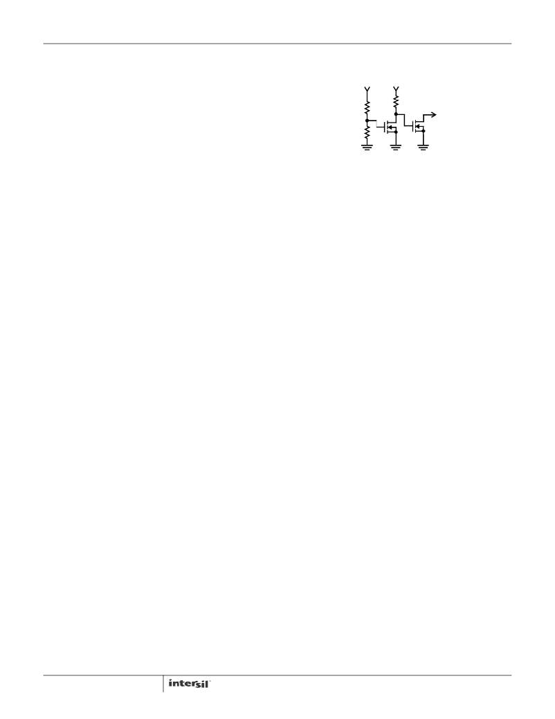
�FIGURE� 6.� SEQUENCER� CIRCUIT�
�(� R� S� +� R� O� )�
�V� OUT� =� 0.6V� ?� ---------------------------�
�R� O� =� ----------------------------------�
�R� O�
�R� S� ?� 0.6V�
�V� OUT� –� 0.6V�
�(EQ.� 2)�
�The� V� IN� range� can� be� as� low� as� ~1V� (for� V� OUT� as� low� as� the�
�0.6V� reference).� It� can� be� as� high� as� 20V� (for� V� OUT� just�
�below� V� IN� ).� There� are� some� restrictions� for� running� high� V� IN�
�voltage.�
�Input� Voltage� Considerations�
�The� Typical� Application� diagram� on� page� 3� shows� a�
�standard� configuration� where� V� CC� is� either� 5V� (±10%)� or�
�12V� (±20%);� in� each� case,� the� gate� drivers� use� the� V� CC�
�voltage� for� LGATE� and� BOOT/UGATE.� In� addition,� V� CC� is�
�allowed� to� work� anywhere� from� 6.5V� up� to� the� 14.4V�
�maximum.� The� V� CC� range� between� 5.5V� and� 6.5V� is� NOT�
�allowed� for� long-term� reliability� reasons,� but� transitions�
�through� it� to� voltages� above� 6.5V� are� acceptable.�
�There� is� an� internal� 5V� regulator� for� bias;� it� turns� on� between�
�5.5V� and� 6.5V;� some� of� the� delay� after� POR� is� there� to� allow�
�a� typical� power� supply� to� ramp� up� past� 6.5V� before� the�
�soft-start� ramps� begins.� This� prevents� a� disturbance� on� the�
�output,� due� to� the� internal� regulator� turning� on� or� off.� If� the�
�transition� is� slow� (not� a� step� change),� the� disturbance� should�
�be� minimal.� So� while� the� recommendation� is� to� not� have� the�
�output� enabled� during� the� transition� through� this� region,� it�
�may� be� acceptable.� The� user� should� monitor� the� output� for�
�their� application,� to� see� if� there� is� any� problem.�
�The� V� IN� to� the� upper� MOSFET� can� share� the� same� supply�
�as� V� CC� ,� but� can� also� run� off� a� separate� supply� or� other�
�sources,� such� as� outputs� of� other� regulators.� If� V� CC� powers�
�up� first,� and� the� V� IN� is� not� present� by� the� time� the�
�initialization� is� done,� then� the� soft-start� will� not� be� able� to�
�ramp� the� output,� and� the� output� will� later� follow� part� of� the�
�V� IN� ramp� when� it� is� applied.� If� this� is� not� desired,� then�
�change� the� sequencing� of� the� supplies,� or� use� the�
�COMP/SD� pin� to� disable� V� OUT� until� both� supplies� are� ready.�
�Figure� 6� shows� a� simple� sequencer� for� this� situation.� If� V� CC�
�powers� up� first,� Q� 1� will� be� off,� and� R� 3� pulling� to� V� CC� will� turn�
�Q� 2� on,� keeping� the� ISL6545x� in� shut-down.� When� V� IN� turns�
�on,� the� resistor� divider� R� 1� and� R� 2� determines� when� Q� 1� turns�
�on,� which� will� turn� off� Q� 2� ,� and� release� the� shut-down.� If� V� IN�
�powers� up� first,� Q� 1� will� be� on,� turning� Q� 2� off;� so� the�
�ISL6545x� will� start-up� as� soon� as� V� CC� comes� up.� The�
�V� DISABLE� trip� point� is� 0.4V� nominal,� so� a� wide� variety� of�
�NFET’s� or� NPN’s� or� even� some� logic� IC’s� can� be� used� as� Q� 1�
�or� Q� 2� ;� but� Q� 2� must� be� low� leakage� when� off� (open-drain� or�
�9�
�The� first� consideration� for� high� V� IN� is� the� maximum� BOOT�
�voltage� of� 36V.� The� V� IN� (as� seen� on� PHASE)� plus� V� CC� (boot�
�voltage� -� minus� the� diode� drop),� plus� any� ringing� (or� other�
�transients)� on� the� BOOT� pin� must� be� less� than� 36V.� If� V� IN� is�
�20V,� that� limits� V� CC� plus� ringing� to� 16V.�
�The� second� consideration� for� high� V� IN� is� the� maximum�
�(BOOT� -� V� CC� )� voltage;� this� must� be� less� than� 24V.� Since�
�BOOT� =� V� IN� +� V� CC� +� ringing,� that� reduces� to� (V� IN� +� ringing)�
�must� be� <24V.� So� based� on� typical� circuits,� a� 20V� maximum�
�V� IN� is� a� good� starting� assumption;� the� user� should� verify� the�
�ringing� in� their� particular� application.�
�Another� consideration� for� high� V� IN� is� duty� cycle.� Very� low�
�duty� cycles� (such� as� 20V� in� to� 1.0V� out,� for� 5%� duty� cycle)�
�require� component� selection� compatible� with� that� choice�
�(such� as� low� r� DS(ON)� lower� MOSFET,� and� a� good� LC� output�
�filter).� At� the� other� extreme� (for� example,� 20V� in� to� 12V� out),�
�the� upper� MOSFET� needs� to� be� low� r� DS(ON)� .� In� addition,� if�
�the� duty� cycle� gets� too� high,� it� can� affect� the� overcurrent�
�sample� time.� In� all� cases,� the� input� and� output� capacitors�
�and� both� MOSFETs� must� be� rated� for� the� voltages� present.�
�Switching� Frequency�
�The� switching� frequency� is� either� a� fixed� 300kHz� or� 600kHz,�
�depending� on� the� part� number� chosen� (ISL6545� is� 300kHz;�
�ISL6545A� is� 600kHz).� However,� all� of� the� other� timing�
�mentioned� (POR� delay,� OCP� sample,� soft-start,� etc.)� is�
�independent� of� the� clock� frequency,� unless� otherwise� noted.�
�BOOT� Refresh�
�In� the� event� that� the� UGATE� is� on� for� an� extended� period� of�
�time,� the� charge� on� the� boot� capacitor� can� start� to� sag,�
�raising� the� r� DS(ON)� of� the� upper� MOSFET.� The� ISL6545x�
�has� a� circuit� that� detects� a� long� UGATE� on-time� (nominal�
�100μs),� and� forces� the� LGATE� to� go� high� for� one� clock� cycle,�
�which� will� allow� the� boot� capacitor� some� time� to� recharge.�
�Separately,� the� OCP� circuit� has� an� LGATE� pulse� stretcher�
�(to� be� sure� the� sample� time� is� long� enough),� which� can� also�
�help� refresh� the� boot.� But� if� OCP� is� disabled� (no� current�
�FN6305.6�
�March� 3,� 2011�
�相关PDF资料 |
PDF描述 |
|---|---|
| ISL6548ACRZA-T | IC REG/CTLR ACPI DUAL DDR 28QFN |
| ISL6548CRZA | IC REG/CTRLR ACPI DUAL DDR 28QFN |
| ISL6551IR-T | IC REG CTRLR FLYBACK PWM 28-QFN |
| ISL6552CR-T | IC REG CTRLR BUCK PWM 20-QFN |
| ISL6553CB-T | IC REG CTRLR BUCK PWM 16-SOIC |
相关代理商/技术参数 |
参数描述 |
|---|---|
| ISL6545IRZ | 功能描述:IC REG CTRLR BUCK PWM VM 10-DFN RoHS:是 类别:集成电路 (IC) >> PMIC - 稳压器 - DC DC 切换控制器 系列:- 产品培训模块:Lead (SnPb) Finish for COTS Obsolescence Mitigation Program 标准包装:2,500 系列:- PWM 型:电流模式 输出数:1 频率 - 最大:275kHz 占空比:50% 电源电压:18 V ~ 110 V 降压:无 升压:无 回扫:无 反相:无 倍增器:无 除法器:无 Cuk:无 隔离:是 工作温度:-40°C ~ 85°C 封装/外壳:8-SOIC(0.154",3.90mm 宽) 包装:带卷 (TR) |
| ISL6545IRZ-T | 功能描述:IC REG CTRLR BUCK PWM VM 10-DFN RoHS:是 类别:集成电路 (IC) >> PMIC - 稳压器 - DC DC 切换控制器 系列:- 产品培训模块:Lead (SnPb) Finish for COTS Obsolescence Mitigation Program 标准包装:2,500 系列:- PWM 型:电流模式 输出数:1 频率 - 最大:275kHz 占空比:50% 电源电压:18 V ~ 110 V 降压:无 升压:无 回扫:无 反相:无 倍增器:无 除法器:无 Cuk:无 隔离:是 工作温度:-40°C ~ 85°C 封装/外壳:8-SOIC(0.154",3.90mm 宽) 包装:带卷 (TR) |
| ISL6546IRZ | 功能描述:IC REG BUCK SYNC 1.2A 10-QFN RoHS:是 类别:集成电路 (IC) >> PMIC - 稳压器 - DC DC 开关稳压器 系列:- 产品培训模块:Lead (SnPb) Finish for COTS Obsolescence Mitigation Program 标准包装:1 系列:- 类型:降压(降压) 输出类型:固定 输出数:1 输出电压:3.3V 输入电压:4.5 V ~ 24 V PWM 型:- 频率 - 开关:- 电流 - 输出:125mA 同步整流器:无 工作温度:-40°C ~ 85°C 安装类型:表面贴装 封装/外壳:SOT-23-6 包装:Digi-Reel® 供应商设备封装:SOT-6 其它名称:MAX1836EUT33#TG16DKR |
| ISL6546IRZ-T | 功能描述:IC REG BUCK SYNC 1.2A 10-QFN RoHS:是 类别:集成电路 (IC) >> PMIC - 稳压器 - DC DC 开关稳压器 系列:- 产品培训模块:Lead (SnPb) Finish for COTS Obsolescence Mitigation Program 标准包装:1 系列:- 类型:降压(降压) 输出类型:固定 输出数:1 输出电压:3.3V 输入电压:4.5 V ~ 24 V PWM 型:- 频率 - 开关:- 电流 - 输出:125mA 同步整流器:无 工作温度:-40°C ~ 85°C 安装类型:表面贴装 封装/外壳:SOT-23-6 包装:Digi-Reel® 供应商设备封装:SOT-6 其它名称:MAX1836EUT33#TG16DKR |
| ISL6548A-6506EVAL1Z | 功能描述:EVALUATION BOARD ISL6548A-6506 RoHS:是 类别:编程器,开发系统 >> 评估板 - DC/DC 与 AC/DC(离线)SMPS 系列:- 产品培训模块:Obsolescence Mitigation Program 标准包装:1 系列:True Shutdown™ 主要目的:DC/DC,步升 输出及类型:1,非隔离 功率 - 输出:- 输出电压:- 电流 - 输出:1A 输入电压:2.5 V ~ 5.5 V 稳压器拓扑结构:升压 频率 - 开关:3MHz 板类型:完全填充 已供物品:板 已用 IC / 零件:MAX8969 |
发布紧急采购,3分钟左右您将得到回复。