参数资料
| 型号: | ISL6566CR |
| 厂商: | Intersil |
| 文件页数: | 21/29页 |
| 文件大小: | 0K |
| 描述: | IC CTRLR PWM BUCK 3PHASE 40-QFN |
| 标准包装: | 50 |
| 应用: | 控制器,Intel VRM9,VRM10,AMD Hammer 应用 |
| 输入电压: | 3 V ~ 12 V |
| 输出数: | 1 |
| 输出电压: | 0.8 V ~ 1.6 V |
| 工作温度: | 0°C ~ 70°C |
| 安装类型: | 表面贴装 |
| 封装/外壳: | 40-VFQFN 裸露焊盘 |
| 供应商设备封装: | 40-QFN(6x6) |
| 包装: | 管件 |
第1页第2页第3页第4页第5页第6页第7页第8页第9页第10页第11页第12页第13页第14页第15页第16页第17页第18页第19页第20页当前第21页第22页第23页第24页第25页第26页第27页第28页第29页
�� �
�
�ISL6566�
�P� UP� ,� 1� ≈� V� IN� ?� ------� +� ---------� ?� ?� ----� 1� ?� f� S�
�P� Qg_TOT� =� P� Qg_Q1� +� P� Qg_Q2� +� I� Q� ?� VCC�
�P� Qg_Q1� =� ---� ?� Q� G1� ?� PVCC� ?� F� SW� ?� N� Q1� ?� N� PHASE�
�UPPER� MOSFET� POWER� CALCULATION�
�In� addition� to� r� DS(ON)� losses,� a� large� portion� of� the� upper-�
�MOSFET� losses� are� due� to� currents� conducted� across� the�
�input� voltage� (V� IN� )� during� switching.� Since� a� substantially�
�higher� portion� of� the� upper-MOSFET� losses� are� dependent�
�on� switching� frequency,� the� power� calculation� is� more�
�complex.� Upper� MOSFET� losses� can� be� divided� into�
�separate� components� involving� the� upper-MOSFET�
�switching� times,� the� lower-MOSFET� body-diode� reverse-�
�recovery� charge,� Q� rr� ,� and� the� upper� MOSFET� r� DS(ON)�
�conduction� loss.�
�When� the� upper� MOSFET� turns� off,� the� lower� MOSFET� does�
�not� conduct� any� portion� of� the� inductor� current� until� the�
�voltage� at� the� phase� node� falls� below� ground.� Once� the�
�lower� MOSFET� begins� conducting,� the� current� in� the� upper�
�MOSFET� falls� to� zero� as� the� current� in� the� lower� MOSFET�
�ramps� up� to� assume� the� full� inductor� current.� In� Equation� 17,�
�the� required� time� for� this� commutation� is� t� 1� and� the�
�approximated� associated� power� loss� is� P� UP,1� .�
�I� M� I� PP� ?� t� ?� (EQ.� 17)�
�?� N� 2� ?� ?� 2� ?�
�At� turn� on,� the� upper� MOSFET� begins� to� conduct� and� this�
�by� all� three� drivers� must� be� less� than� the� maximum�
�allowable� power� dissipation� for� the� QFN� package.�
�Calculating� the� power� dissipation� in� the� drivers� for� a� desired�
�application� is� critical� to� ensure� safe� operation.� Exceeding� the�
�maximum� allowable� power� dissipation� level� will� push� the� IC�
�beyond� the� maximum� recommended� operating� junction�
�temperature� of� 125°C.� The� maximum� allowable� IC� power�
�dissipation� for� the� 6x6� QFN� package� is� approximately� 4W� at�
�room� temperature.� See� Layout� Considerations� paragraph� for�
�thermal� transfer� improvement� suggestions.�
�When� designing� the� ISL6566� into� an� application,� it� is�
�recommended� that� the� following� calculation� is� used� to�
�ensure� safe� operation� at� the� desired� frequency� for� the�
�selected� MOSFETs.� The� total� gate� drive� power� losses,�
�P� Qg_TOT� ,� due� to� the� gate� charge� of� MOSFETs� and� the�
�integrated� driver� ’s� internal� circuitry� and� their� corresponding�
�average� driver� current� can� be� estimated� with� Equations� 21�
�and� 22,� respectively.�
�(EQ.� 21)�
�3�
�2�
�P� UP� ,� 2� ≈� V� IN� ?� ------� –� ---------� ?� ?� ----� 2� ?� f� S�
�I� DR� =� ?� ---� ?� Q� G1� ?� N�
�+� Q� G2� ?� N� Q2� ?� ?� N� PHASE� ?� F� SW� +� I� Q�
�transition� occurs� over� a� time� t� 2� .� In� Equation� 18,� the�
�approximate� power� loss� is� P� UP,2� .�
�I� M� I� PP� ?� t� ?�
�?� N� 2� ?� ?� 2� ?�
�(EQ.� 18)�
�P� Qg_Q2� =� Q� G2� ?� PVCC� ?� F� SW� ?� N� Q2� ?� N� PHASE�
�3�
�?� 2� Q1� ?�
�P� UP� ,� 3� =� V� IN� Q� rr� f� S�
�I� PP2�
�?� I� M� ?�
�P� UP� ,� 4� ≈� r� DS� (� ON� )� ?� ------� ?� d� +� ----------�
�A� third� component� involves� the� lower� MOSFET� reverse-�
�recovery� charge,� Q� rr� .� Since� the� inductor� current� has� fully�
�commutated� to� the� upper� MOSFET� before� the� lower-�
�MOSFET� body� diode� can� recover� all� of� Q� rr� ,� it� is� conducted�
�through� the� upper� MOSFET� across� VIN.� The� power�
�dissipated� as� a� result� is� P� UP,3� .�
�(EQ.� 19)�
�Finally,� the� resistive� part� of� the� upper� MOSFET� is� given� in�
�Equation� 20� as� P� UP,4� .�
�2�
�(EQ.� 20)�
�?� N� ?� 12�
�(EQ.� 22)�
�In� Equations� 21� and� 22,� P� Qg_Q1� is� the� total� upper� gate� drive�
�power� loss� and� P� Qg_Q2� is� the� total� lower� gate� drive� power�
�loss;� the� gate� charge� (Q� G1� and� Q� G2� )� is� defined� at� the�
�particular� gate� to� source� drive� voltage� PVCC� in� the�
�corresponding� MOSFET� data� sheet;� I� Q� is� the� driver� total�
�quiescent� current� with� no� load� at� both� drive� outputs;� N� Q1�
�and� N� Q2� are� the� number� of� upper� and� lower� MOSFETs� per�
�phase,� respectively;� N� PHASE� is� the� number� of� active�
�phases.� The� I� Q*� VCC� product� is� the� quiescent� power� of� the�
�controller� without� capacitive� load� and� is� typically� 75mW� at�
�300kHz.�
�The� total� power� dissipated� by� the� upper� MOSFET� at� full� load�
�can� now� be� approximated� as� the� summation� of� the� results�
�from� Equations� 17,� 18,� 19� and� 20.� Since� the� power�
�equations� depend� on� MOSFET� parameters,� choosing� the�
�correct� MOSFETs� can� be� an� iterative� process� involving�
�repetitive� solutions� to� the� loss� equations� for� different�
�MOSFETs� and� different� switching� frequencies.�
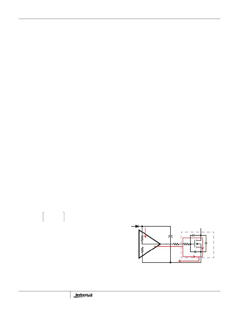
�PVCC�
�BOOT�
�R� HI1�
�R� LO1�
�UGATE�
�G�
�R� G1�
�C� GD�
�R� GI1�
�C� GS�
�D�
�C� DS�
�Q1�
�Package� Power� Dissipation�
�When� choosing� MOSFETs� it� is� important� to� consider� the�
�amount� of� power� being� dissipated� in� the� integrated� drivers�
�located� in� the� controller.� Since� there� are� a� total� of� three�
�drivers� in� the� controller� package,� the� total� power� dissipated�
�21�
�S�
�PHASE�
�FIGURE� 15.� TYPICAL� UPPER-GATE� DRIVE� TURN-ON� PATH�
�FN9178.4�
�March� 9,� 2006�
�相关PDF资料 |
PDF描述 |
|---|---|
| X5168S8I-2.7AT1 | IC SUPERVISOR CPU 16K EE 8-SOIC |
| ECC44DRES-S734 | CONN EDGECARD 88POS .100 EYELET |
| ISL6563CR-T | IC CTRLR PWM MULTIPHASE 24-QFN |
| ISL6563CR | IC CTRLR PWM MULTIPHASE 24-QFN |
| X5168S8I-2.7 | IC SUPERVISOR CPU 16K EE 8-SOIC |
相关代理商/技术参数 |
参数描述 |
|---|---|
| ISL6566CRR5184 | 制造商:Rochester Electronics LLC 功能描述: 制造商:Intersil Corporation 功能描述: |
| ISL6566CR-T | 功能描述:IC CTRLR PWM BUCK 3PHASE 40-QFN RoHS:否 类别:集成电路 (IC) >> PMIC - 稳压器 - 专用型 系列:- 产品培训模块:Lead (SnPb) Finish for COTS Obsolescence Mitigation Program 标准包装:2,000 系列:- 应用:电源,ICERA E400,E450 输入电压:4.1 V ~ 5.5 V 输出数:10 输出电压:可编程 工作温度:-40°C ~ 85°C 安装类型:表面贴装 封装/外壳:42-WFBGA,WLCSP 供应商设备封装:42-WLP 包装:带卷 (TR) |
| ISL6566CRZ | 功能描述:IC CTRLR PWM BUCK 3PHASE 40QFN RoHS:是 类别:集成电路 (IC) >> PMIC - 稳压器 - 专用型 系列:- 产品培训模块:Lead (SnPb) Finish for COTS Obsolescence Mitigation Program 标准包装:2,000 系列:- 应用:电源,ICERA E400,E450 输入电压:4.1 V ~ 5.5 V 输出数:10 输出电压:可编程 工作温度:-40°C ~ 85°C 安装类型:表面贴装 封装/外壳:42-WFBGA,WLCSP 供应商设备封装:42-WLP 包装:带卷 (TR) |
| ISL6566CRZA | 制造商:Intersil Corporation 功能描述:CURRENT MODE PWM CNTRLR 0.8375V TO 1.6V 100A 40QFN EP - Rail/Tube |
| ISL6566CRZAR5184 | 功能描述:IC CTRLR PWM 3PHASE BUCK 40-QFN RoHS:是 类别:集成电路 (IC) >> PMIC - 稳压器 - 专用型 系列:- 标准包装:43 系列:- 应用:控制器,Intel VR11 输入电压:5 V ~ 12 V 输出数:1 输出电压:0.5 V ~ 1.6 V 工作温度:-40°C ~ 85°C 安装类型:表面贴装 封装/外壳:48-VFQFN 裸露焊盘 供应商设备封装:48-QFN(7x7) 包装:管件 |
发布紧急采购,3分钟左右您将得到回复。