- 您现在的位置:买卖IC网 > PDF目录4568 > LFX125EB-05F256C (Lattice Semiconductor Corporation)IC FPGA 139K GATES 256-BGA PDF资料下载
参数资料
| 型号: | LFX125EB-05F256C |
| 厂商: | Lattice Semiconductor Corporation |
| 文件页数: | 2/119页 |
| 文件大小: | 0K |
| 描述: | IC FPGA 139K GATES 256-BGA |
| 标准包装: | 90 |
| 系列: | ispXPGA® |
| 逻辑元件/单元数: | 1936 |
| RAM 位总计: | 94208 |
| 输入/输出数: | 160 |
| 门数: | 139000 |
| 电源电压: | 2.3 V ~ 3.6 V |
| 安装类型: | 表面贴装 |
| 工作温度: | 0°C ~ 85°C |
| 封装/外壳: | 256-BGA |
| 供应商设备封装: | 256-FPBGA(17x17) |
第1页当前第2页第3页第4页第5页第6页第7页第8页第9页第10页第11页第12页第13页第14页第15页第16页第17页第18页第19页第20页第21页第22页第23页第24页第25页第26页第27页第28页第29页第30页第31页第32页第33页第34页第35页第36页第37页第38页第39页第40页第41页第42页第43页第44页第45页第46页第47页第48页第49页第50页第51页第52页第53页第54页第55页第56页第57页第58页第59页第60页第61页第62页第63页第64页第65页第66页第67页第68页第69页第70页第71页第72页第73页第74页第75页第76页第77页第78页第79页第80页第81页第82页第83页第84页第85页第86页第87页第88页第89页第90页第91页第92页第93页第94页第95页第96页第97页第98页第99页第100页第101页第102页第103页第104页第105页第106页第107页第108页第109页第110页第111页第112页第113页第114页第115页第116页第117页第118页第119页
Lattice Semiconductor
ispXPGA Family Data Sheet
6
Configurable Logic Element
The CLE is made up of a four-input Look-up Table (LUT-4), a Carry Chain Generator (CCG), and a two-input AND
gate. The LUT-4 creates various combinatorial and memory elements, the CCG creates a single one-bit full adder,
and the two-input AND gate can expand the CCG to incorporate Booth Multiplier capability by feeding the output of
the AND gate to one of the inputs of the CCG.
Of the five inputs that feed each CLE, two are dedicated inputs into each LUT-4 and the remaining three take on
varying functionality. The third and fourth inputs can be used as either inputs to the LUT-4 or as a Feed-Thru to the
CSE via the WLG. The fifth input can be a data port when the LUT is configured as Distributed Memory, a select
line for multiplexer operation, or a Feed-Thru directly to the CSE via the WLG (Figure 2).
Look-Up Table – Combinatorial Mode
In combinatorial mode, the LUT-4 can implement any logic function up to four inputs. By using the carry chain and
the WLG, each LUT-4 can be combined to form the enhanced functions listed in Table 3.
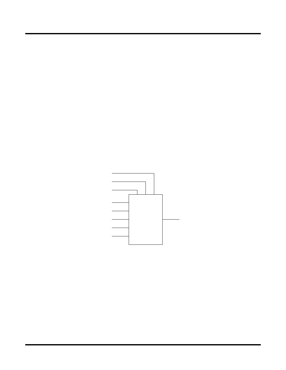
Look-Up Table – Distributed Memory Mode
In the distributed memory mode, the LUT functions as a memory element. The inputs to the LUT function as
Address and Data. Each PFU is capable of implementing up to 64 SRAM bits. Both single and double port RAM
can be performed in the PFU (Table 3). Furthermore, the distributed memory can be configured as either synchro-
nous or asynchronous memory. Figure 3 illustrates the LUT while in distributed memory mode. When using any
LUT in the PFU in memory mode, the Set/Reset signal will be used for Write Enable (WE(SR)) and the CLK0 signal
will be used as the clock for synchronous read and write.
Figure 3. LUT in Distributed Memory Mode
Look-Up Table – Shift Register Mode
In the shift register mode, the LUT functions as a 1-bit to 8-bit shift register. This means that each PFU can imple-
ment up to four 8-bit shift registers or any cascaded combination. Figure 4 illustrates the LUT when configured in
shift register mode.
LUT-4
ADDR[0] (IN0)
PFUCLK0
ADDR[1] (IN1)
ADDR[2] (IN2)
ADDR[3] (IN3)
CEB0
WE (SR)
DOUT (4A)
DIN (SEL)
SELECT
DEVICES
DISCONTINUED
相关PDF资料 |
PDF描述 |
|---|---|
| LFX125EB-05FN256C | IC FPGA 139K GATES 256-BGA |
| MAX9950DCCB+D | IC PPMU DUAL SPI 64TQFP |
| LFX125EB-04FN256I | IC FPGA 139K GATES 256-BGA |
| MAX9949DCCB+D | IC PPMU DUAL SPI 64TQFP |
| DS1402D-DR8+ | CABLE 8' BLUE DOT TO RJ11 |
相关代理商/技术参数 |
参数描述 |
|---|---|
| LFX125EB-05F516C | 功能描述:FPGA - 现场可编程门阵列 139K 176 I/O ispJTAG RoHS:否 制造商:Altera Corporation 系列:Cyclone V E 栅极数量: 逻辑块数量:943 内嵌式块RAM - EBR:1956 kbit 输入/输出端数量:128 最大工作频率:800 MHz 工作电源电压:1.1 V 最大工作温度:+ 70 C 安装风格:SMD/SMT 封装 / 箱体:FBGA-256 |
| LFX125EB-05FH516C | 功能描述:FPGA - 现场可编程门阵列 Use LFX125EB-05F516C RoHS:否 制造商:Altera Corporation 系列:Cyclone V E 栅极数量: 逻辑块数量:943 内嵌式块RAM - EBR:1956 kbit 输入/输出端数量:128 最大工作频率:800 MHz 工作电源电压:1.1 V 最大工作温度:+ 70 C 安装风格:SMD/SMT 封装 / 箱体:FBGA-256 |
| LFX125EB-05FN256C | 功能描述:FPGA - 现场可编程门阵列 E-Ser139K Gt ispJTAG 2.5/3.3V -5 Spd RoHS:否 制造商:Altera Corporation 系列:Cyclone V E 栅极数量: 逻辑块数量:943 内嵌式块RAM - EBR:1956 kbit 输入/输出端数量:128 最大工作频率:800 MHz 工作电源电压:1.1 V 最大工作温度:+ 70 C 安装风格:SMD/SMT 封装 / 箱体:FBGA-256 |
| LFX125EB-05FN516C | 功能描述:FPGA - 现场可编程门阵列 E-Ser139K Gt ispJTA G 2.5/3.3V -5 Spd RoHS:否 制造商:Altera Corporation 系列:Cyclone V E 栅极数量: 逻辑块数量:943 内嵌式块RAM - EBR:1956 kbit 输入/输出端数量:128 最大工作频率:800 MHz 工作电源电压:1.1 V 最大工作温度:+ 70 C 安装风格:SMD/SMT 封装 / 箱体:FBGA-256 |
| LFX125EB-3F256C | 制造商:LATTICE 制造商全称:Lattice Semiconductor 功能描述:ispXPGA Family |
发布紧急采购,3分钟左右您将得到回复。