- 您现在的位置:买卖IC网 > PDF目录4568 > LFX125EB-05F256C (Lattice Semiconductor Corporation)IC FPGA 139K GATES 256-BGA PDF资料下载
参数资料
| 型号: | LFX125EB-05F256C |
| 厂商: | Lattice Semiconductor Corporation |
| 文件页数: | 31/119页 |
| 文件大小: | 0K |
| 描述: | IC FPGA 139K GATES 256-BGA |
| 标准包装: | 90 |
| 系列: | ispXPGA® |
| 逻辑元件/单元数: | 1936 |
| RAM 位总计: | 94208 |
| 输入/输出数: | 160 |
| 门数: | 139000 |
| 电源电压: | 2.3 V ~ 3.6 V |
| 安装类型: | 表面贴装 |
| 工作温度: | 0°C ~ 85°C |
| 封装/外壳: | 256-BGA |
| 供应商设备封装: | 256-FPBGA(17x17) |
第1页第2页第3页第4页第5页第6页第7页第8页第9页第10页第11页第12页第13页第14页第15页第16页第17页第18页第19页第20页第21页第22页第23页第24页第25页第26页第27页第28页第29页第30页当前第31页第32页第33页第34页第35页第36页第37页第38页第39页第40页第41页第42页第43页第44页第45页第46页第47页第48页第49页第50页第51页第52页第53页第54页第55页第56页第57页第58页第59页第60页第61页第62页第63页第64页第65页第66页第67页第68页第69页第70页第71页第72页第73页第74页第75页第76页第77页第78页第79页第80页第81页第82页第83页第84页第85页第86页第87页第88页第89页第90页第91页第92页第93页第94页第95页第96页第97页第98页第99页第100页第101页第102页第103页第104页第105页第106页第107页第108页第109页第110页第111页第112页第113页第114页第115页第116页第117页第118页第119页
Lattice Semiconductor
ispXPGA Family Data Sheet
15
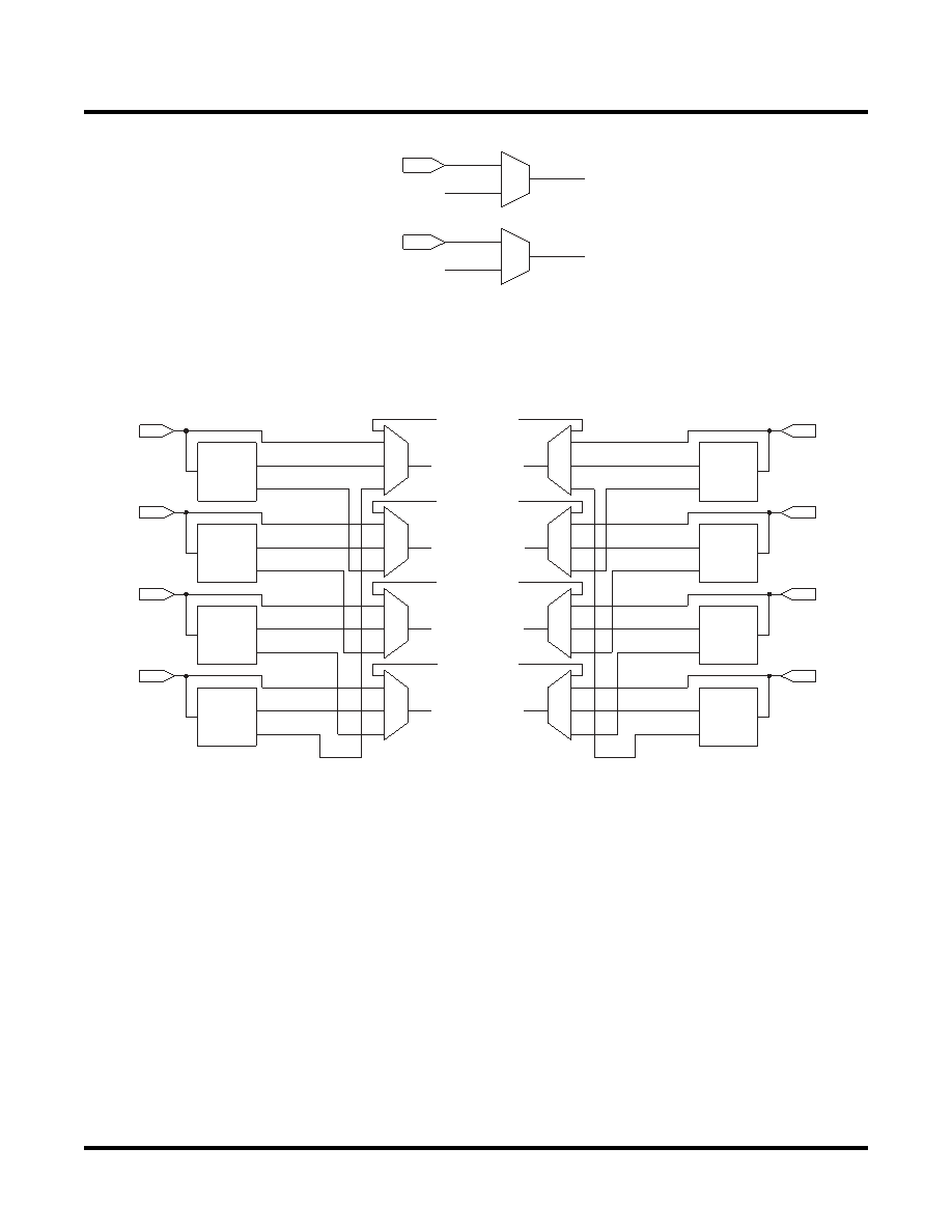
Figure 17. ispXPGA PLL_RST and PLL_FBK Generation
Clock Routing
The Global Clock Lines (GCLK) have two sources, their dedicated pins and the sysCLOCK circuit. Figure 18 illus-
trates the generation of the Global Clock Lines.
Figure 18. Global Clock Line Generation
sysIO Capability
All the ispXPGA devices have eight sysIO banks, where each bank is capable of supporting multiple I/O standards.
Each sysIO bank has its own I/O supply voltage (VCCO) and reference voltage (VREF) resources allowing each
bank complete independence from the others. Each I/O is individually configurable based on the bank’s VCCO and
VREF settings. In addition, each I/O has configurable drive strength, weak pull-up, weak pull-down, or a bus-keeper
latch. Table 4 lists the number of I/Os supported per bank in each of the ispXPGA devices. In addition, 5V tolerant
inputs are specified within an I/O bank that is connected to VCCO of 3.0V to 3.6V for LVCMOS 3.3, LVTTL and PCI
interfaces.
The TOE, JTAG TAP pins, PROGRAM, CFG0 and DONE pins of the ispXPGA device are the only pins that do not
have the sysIO capabilities. The TOE and CFG0 pins operate off the VCC of the device, supporting only the LVC-
MOS standard corresponding to the device supply voltage. The TAP pins have a separate supply voltage (VCCJ),
which determines the LVCMOS standard corresponding to that supply voltage.
There are three classes of I/O interface standards that are implemented in the ispXPGA devices. The first is the un-
terminated, single-ended interface. It includes the 3.3V LVTTL standard along with the 1.8V, 2.5V, and 3.3V LVC-
MOS interface standards. Additionally, PCI and AGP-1X are subsets of this type of interface.
I/O/PLL_RST
I/O/PLL_FBK
From Routing
From Clock Net
To PLL
PLL0
GCLK0
CLK_OUT0
SEC_OUT0
PLL1
CLK_OUT1
SEC_OUT1
GCLK1
PLL2
CLK_OUT2
SEC_OUT2
GCLK2
PLL3
CLK_OUT3
SEC_OUT3
GCLK3
PLL7
GCLK7
CLK_OUT7
SEC_OUT7
PLL6
CLK_OUT6
SEC_OUT6
GCLK6
PLL5
CLK_OUT5
SEC_OUT5
GCLK5
PLL4
CLK_OUT4
SEC_OUT4
GCLK4
CLK0
CLK1
CLK2
CLK3
CLK7
CLK6
CLK5
CLK4
From Routing
DEVICES
DISCONTINUED
相关PDF资料 |
PDF描述 |
|---|---|
| LFX125EB-05FN256C | IC FPGA 139K GATES 256-BGA |
| MAX9950DCCB+D | IC PPMU DUAL SPI 64TQFP |
| LFX125EB-04FN256I | IC FPGA 139K GATES 256-BGA |
| MAX9949DCCB+D | IC PPMU DUAL SPI 64TQFP |
| DS1402D-DR8+ | CABLE 8' BLUE DOT TO RJ11 |
相关代理商/技术参数 |
参数描述 |
|---|---|
| LFX125EB-05F516C | 功能描述:FPGA - 现场可编程门阵列 139K 176 I/O ispJTAG RoHS:否 制造商:Altera Corporation 系列:Cyclone V E 栅极数量: 逻辑块数量:943 内嵌式块RAM - EBR:1956 kbit 输入/输出端数量:128 最大工作频率:800 MHz 工作电源电压:1.1 V 最大工作温度:+ 70 C 安装风格:SMD/SMT 封装 / 箱体:FBGA-256 |
| LFX125EB-05FH516C | 功能描述:FPGA - 现场可编程门阵列 Use LFX125EB-05F516C RoHS:否 制造商:Altera Corporation 系列:Cyclone V E 栅极数量: 逻辑块数量:943 内嵌式块RAM - EBR:1956 kbit 输入/输出端数量:128 最大工作频率:800 MHz 工作电源电压:1.1 V 最大工作温度:+ 70 C 安装风格:SMD/SMT 封装 / 箱体:FBGA-256 |
| LFX125EB-05FN256C | 功能描述:FPGA - 现场可编程门阵列 E-Ser139K Gt ispJTAG 2.5/3.3V -5 Spd RoHS:否 制造商:Altera Corporation 系列:Cyclone V E 栅极数量: 逻辑块数量:943 内嵌式块RAM - EBR:1956 kbit 输入/输出端数量:128 最大工作频率:800 MHz 工作电源电压:1.1 V 最大工作温度:+ 70 C 安装风格:SMD/SMT 封装 / 箱体:FBGA-256 |
| LFX125EB-05FN516C | 功能描述:FPGA - 现场可编程门阵列 E-Ser139K Gt ispJTA G 2.5/3.3V -5 Spd RoHS:否 制造商:Altera Corporation 系列:Cyclone V E 栅极数量: 逻辑块数量:943 内嵌式块RAM - EBR:1956 kbit 输入/输出端数量:128 最大工作频率:800 MHz 工作电源电压:1.1 V 最大工作温度:+ 70 C 安装风格:SMD/SMT 封装 / 箱体:FBGA-256 |
| LFX125EB-3F256C | 制造商:LATTICE 制造商全称:Lattice Semiconductor 功能描述:ispXPGA Family |
发布紧急采购,3分钟左右您将得到回复。