- 您现在的位置:买卖IC网 > PDF目录4568 > LFX125EB-05F256C (Lattice Semiconductor Corporation)IC FPGA 139K GATES 256-BGA PDF资料下载
参数资料
| 型号: | LFX125EB-05F256C |
| 厂商: | Lattice Semiconductor Corporation |
| 文件页数: | 33/119页 |
| 文件大小: | 0K |
| 描述: | IC FPGA 139K GATES 256-BGA |
| 标准包装: | 90 |
| 系列: | ispXPGA® |
| 逻辑元件/单元数: | 1936 |
| RAM 位总计: | 94208 |
| 输入/输出数: | 160 |
| 门数: | 139000 |
| 电源电压: | 2.3 V ~ 3.6 V |
| 安装类型: | 表面贴装 |
| 工作温度: | 0°C ~ 85°C |
| 封装/外壳: | 256-BGA |
| 供应商设备封装: | 256-FPBGA(17x17) |
第1页第2页第3页第4页第5页第6页第7页第8页第9页第10页第11页第12页第13页第14页第15页第16页第17页第18页第19页第20页第21页第22页第23页第24页第25页第26页第27页第28页第29页第30页第31页第32页当前第33页第34页第35页第36页第37页第38页第39页第40页第41页第42页第43页第44页第45页第46页第47页第48页第49页第50页第51页第52页第53页第54页第55页第56页第57页第58页第59页第60页第61页第62页第63页第64页第65页第66页第67页第68页第69页第70页第71页第72页第73页第74页第75页第76页第77页第78页第79页第80页第81页第82页第83页第84页第85页第86页第87页第88页第89页第90页第91页第92页第93页第94页第95页第96页第97页第98页第99页第100页第101页第102页第103页第104页第105页第106页第107页第108页第109页第110页第111页第112页第113页第114页第115页第116页第117页第118页第119页
Lattice Semiconductor
ispXPGA Family Data Sheet
16
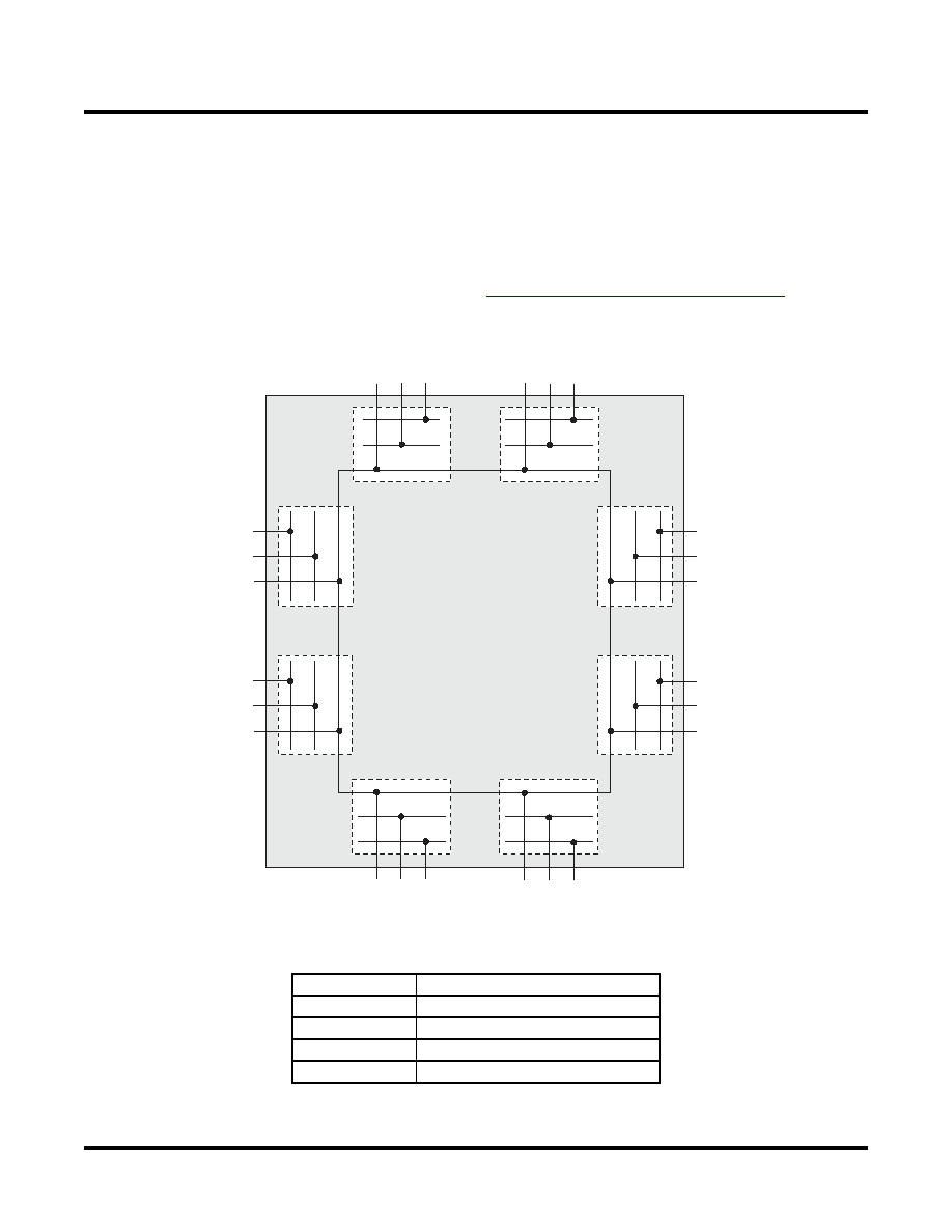
The second type of interface implemented is the terminated, single-ended interface standard. This group of inter-
faces includes different versions of SSTL and HSTL interfaces along with CTT, and GTL+. Usage of these particu-
lar I/O interfaces requires an additional VREF signal. At the system level a termination voltage, VTT, is also required.
Typically an output will be terminated to VTT at the receiving end of the transmission line it is driving.
The third type of interface standards are the differential standards LVDS, BLVDS, and LVPECL. The differential
standards require two I/O pins to create the differential pair. The logic level is determined by the difference in the
two signals. Table 6 lists how these interface standards are implemented in the ispXPGA devices.
For more information on sysIO capability, refer to TN1000, sysIO Usage Guidelines for Lattice Devices.
Figure 19. sysIO Banks per Device
Table 4. Number of I/Os per Bank
Device
Max. Number of I/Os per Bank (N)
XPGA 1200
62
XPGA 500
42
XPGA 200
26
XPGA 125
22
GND
VCCO0
VREF0
GND
VCCO1
VREF1
GND
VCCO5
VREF5
GND
VCCO4
VREF4
GND
V
CCO3
V
REF3
GND
V
CCO2
V
REF2
GND
V
CCO6
V
REF6
GND
I/O
0
I/O
N
I/O 0
I/O N
I/O 0
I/O
0
I/O
N
I/O
N
I/O
0
I/O
N
I/O
0
V
CCO7
V
REF7
Bank 3
Bank 2
Bank 6
Bank 7
Bank
0
Bank
1
Bank
5
Bank
4
SELECT
DEVICES
DISCONTINUED
相关PDF资料 |
PDF描述 |
|---|---|
| LFX125EB-05FN256C | IC FPGA 139K GATES 256-BGA |
| MAX9950DCCB+D | IC PPMU DUAL SPI 64TQFP |
| LFX125EB-04FN256I | IC FPGA 139K GATES 256-BGA |
| MAX9949DCCB+D | IC PPMU DUAL SPI 64TQFP |
| DS1402D-DR8+ | CABLE 8' BLUE DOT TO RJ11 |
相关代理商/技术参数 |
参数描述 |
|---|---|
| LFX125EB-05F516C | 功能描述:FPGA - 现场可编程门阵列 139K 176 I/O ispJTAG RoHS:否 制造商:Altera Corporation 系列:Cyclone V E 栅极数量: 逻辑块数量:943 内嵌式块RAM - EBR:1956 kbit 输入/输出端数量:128 最大工作频率:800 MHz 工作电源电压:1.1 V 最大工作温度:+ 70 C 安装风格:SMD/SMT 封装 / 箱体:FBGA-256 |
| LFX125EB-05FH516C | 功能描述:FPGA - 现场可编程门阵列 Use LFX125EB-05F516C RoHS:否 制造商:Altera Corporation 系列:Cyclone V E 栅极数量: 逻辑块数量:943 内嵌式块RAM - EBR:1956 kbit 输入/输出端数量:128 最大工作频率:800 MHz 工作电源电压:1.1 V 最大工作温度:+ 70 C 安装风格:SMD/SMT 封装 / 箱体:FBGA-256 |
| LFX125EB-05FN256C | 功能描述:FPGA - 现场可编程门阵列 E-Ser139K Gt ispJTAG 2.5/3.3V -5 Spd RoHS:否 制造商:Altera Corporation 系列:Cyclone V E 栅极数量: 逻辑块数量:943 内嵌式块RAM - EBR:1956 kbit 输入/输出端数量:128 最大工作频率:800 MHz 工作电源电压:1.1 V 最大工作温度:+ 70 C 安装风格:SMD/SMT 封装 / 箱体:FBGA-256 |
| LFX125EB-05FN516C | 功能描述:FPGA - 现场可编程门阵列 E-Ser139K Gt ispJTA G 2.5/3.3V -5 Spd RoHS:否 制造商:Altera Corporation 系列:Cyclone V E 栅极数量: 逻辑块数量:943 内嵌式块RAM - EBR:1956 kbit 输入/输出端数量:128 最大工作频率:800 MHz 工作电源电压:1.1 V 最大工作温度:+ 70 C 安装风格:SMD/SMT 封装 / 箱体:FBGA-256 |
| LFX125EB-3F256C | 制造商:LATTICE 制造商全称:Lattice Semiconductor 功能描述:ispXPGA Family |
发布紧急采购,3分钟左右您将得到回复。