- 您现在的位置:买卖IC网 > PDF目录4568 > LFX125EB-05F256C (Lattice Semiconductor Corporation)IC FPGA 139K GATES 256-BGA PDF资料下载
参数资料
| 型号: | LFX125EB-05F256C |
| 厂商: | Lattice Semiconductor Corporation |
| 文件页数: | 27/119页 |
| 文件大小: | 0K |
| 描述: | IC FPGA 139K GATES 256-BGA |
| 标准包装: | 90 |
| 系列: | ispXPGA® |
| 逻辑元件/单元数: | 1936 |
| RAM 位总计: | 94208 |
| 输入/输出数: | 160 |
| 门数: | 139000 |
| 电源电压: | 2.3 V ~ 3.6 V |
| 安装类型: | 表面贴装 |
| 工作温度: | 0°C ~ 85°C |
| 封装/外壳: | 256-BGA |
| 供应商设备封装: | 256-FPBGA(17x17) |
第1页第2页第3页第4页第5页第6页第7页第8页第9页第10页第11页第12页第13页第14页第15页第16页第17页第18页第19页第20页第21页第22页第23页第24页第25页第26页当前第27页第28页第29页第30页第31页第32页第33页第34页第35页第36页第37页第38页第39页第40页第41页第42页第43页第44页第45页第46页第47页第48页第49页第50页第51页第52页第53页第54页第55页第56页第57页第58页第59页第60页第61页第62页第63页第64页第65页第66页第67页第68页第69页第70页第71页第72页第73页第74页第75页第76页第77页第78页第79页第80页第81页第82页第83页第84页第85页第86页第87页第88页第89页第90页第91页第92页第93页第94页第95页第96页第97页第98页第99页第100页第101页第102页第103页第104页第105页第106页第107页第108页第109页第110页第111页第112页第113页第114页第115页第116页第117页第118页第119页
Lattice Semiconductor
ispXPGA Family Data Sheet
11
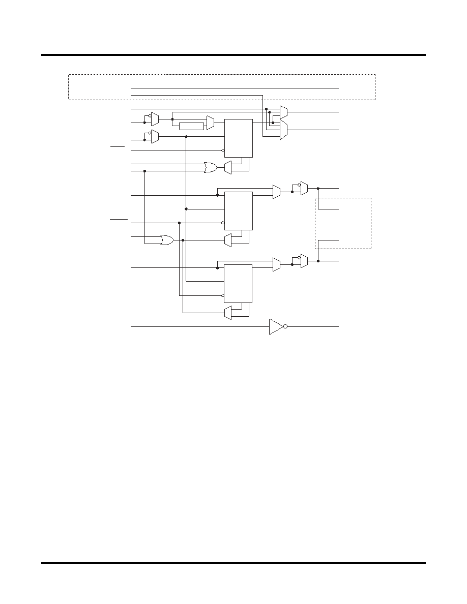
Figure 11. ispXPGA PIO
VLI Routing Resources
The ispXPGA architecture contains a Variable-Length-Interconnect (VLI) routing technology connecting the PFUs,
PICs, and EBRs in the device. There are four types of routing resources, Global Lines, Long Lines, General Inter-
connect, and Local Lines forming the global routing structure. This allows a signal to be routed to any element in
the device with the optimal delay.
The Global Lines consist of global clock lines and a global set/reset line. These lines are routed to all elements in
the device. They are specifically designed for high speed, predictable timing regardless of fan-out. The global clock
lines can also be used as dedicated inputs.
The Long Lines consist of Horizontal and Vertical Long Lines (HLL and VLL). The VLL and HLL are tri-statable
lines spanning the entire device. These lines allow fast routing for high fan-out nets and general-purpose functions.
The General Interconnect consists of Double and Deca Lines. The Double Lines connect up to three elements (two
plus the driving element), while the Deca Lines connect up to eleven elements (ten plus the driving element).
The Local Lines are extremely fast routing paths consisting of Feedback and Direct Connect Lines. The Feedback
Lines are internal routing paths from the PFU outputs to the PFU inputs. The Direct Connect Lines connect all adja-
cent elements.
The Common Interface Block (CIB) provides the link between the logic element (PFU, PIC, or EBR) and the VLI
Routing resources. The CIB is a switch matrix that can be programmed to connect virtually any routing resource to
any input or output of the logic element.
Feed-through (FT)
OUT0
Clock (CLK)
Input Clock Enable (ICEN)
Input Set/Reset (ISR)
Global Set/Reset(GSR)
Output Clock Enable (OCEN)
PIO Input (IN)
Output Set/Reset (OSR)
PIO Output Enable(OEN)
PIO Input Enable (IEN)
OUT1
Delay
OE
From sysIO Input
To sysIO
Output
Enable
To sysIO
Output
CE
DQ
SR
CLK/LE
CE
DQ
SR
CLK/LE
CE
DQ
SR
CLK/LE
From sysHSI block
To Routing
To sysHSI
block
To sysHSI
block
Only for PIOs associated with sysHSI Blocks
Only for PIOs
Associated with
sysHSI Blocks
SELECT
DEVICES
DISCONTINUED
相关PDF资料 |
PDF描述 |
|---|---|
| LFX125EB-05FN256C | IC FPGA 139K GATES 256-BGA |
| MAX9950DCCB+D | IC PPMU DUAL SPI 64TQFP |
| LFX125EB-04FN256I | IC FPGA 139K GATES 256-BGA |
| MAX9949DCCB+D | IC PPMU DUAL SPI 64TQFP |
| DS1402D-DR8+ | CABLE 8' BLUE DOT TO RJ11 |
相关代理商/技术参数 |
参数描述 |
|---|---|
| LFX125EB-05F516C | 功能描述:FPGA - 现场可编程门阵列 139K 176 I/O ispJTAG RoHS:否 制造商:Altera Corporation 系列:Cyclone V E 栅极数量: 逻辑块数量:943 内嵌式块RAM - EBR:1956 kbit 输入/输出端数量:128 最大工作频率:800 MHz 工作电源电压:1.1 V 最大工作温度:+ 70 C 安装风格:SMD/SMT 封装 / 箱体:FBGA-256 |
| LFX125EB-05FH516C | 功能描述:FPGA - 现场可编程门阵列 Use LFX125EB-05F516C RoHS:否 制造商:Altera Corporation 系列:Cyclone V E 栅极数量: 逻辑块数量:943 内嵌式块RAM - EBR:1956 kbit 输入/输出端数量:128 最大工作频率:800 MHz 工作电源电压:1.1 V 最大工作温度:+ 70 C 安装风格:SMD/SMT 封装 / 箱体:FBGA-256 |
| LFX125EB-05FN256C | 功能描述:FPGA - 现场可编程门阵列 E-Ser139K Gt ispJTAG 2.5/3.3V -5 Spd RoHS:否 制造商:Altera Corporation 系列:Cyclone V E 栅极数量: 逻辑块数量:943 内嵌式块RAM - EBR:1956 kbit 输入/输出端数量:128 最大工作频率:800 MHz 工作电源电压:1.1 V 最大工作温度:+ 70 C 安装风格:SMD/SMT 封装 / 箱体:FBGA-256 |
| LFX125EB-05FN516C | 功能描述:FPGA - 现场可编程门阵列 E-Ser139K Gt ispJTA G 2.5/3.3V -5 Spd RoHS:否 制造商:Altera Corporation 系列:Cyclone V E 栅极数量: 逻辑块数量:943 内嵌式块RAM - EBR:1956 kbit 输入/输出端数量:128 最大工作频率:800 MHz 工作电源电压:1.1 V 最大工作温度:+ 70 C 安装风格:SMD/SMT 封装 / 箱体:FBGA-256 |
| LFX125EB-3F256C | 制造商:LATTICE 制造商全称:Lattice Semiconductor 功能描述:ispXPGA Family |
发布紧急采购,3分钟左右您将得到回复。