- 您现在的位置:买卖IC网 > PDF目录15273 > LTC3731CG#TRPBF (Linear Technology)IC REG CTRLR BUCK PWM CM 36-SSOP PDF资料下载
参数资料
| 型号: | LTC3731CG#TRPBF |
| 厂商: | Linear Technology |
| 文件页数: | 15/34页 |
| 文件大小: | 0K |
| 描述: | IC REG CTRLR BUCK PWM CM 36-SSOP |
| 标准包装: | 2,000 |
| 系列: | PolyPhase® |
| PWM 型: | 电流模式 |
| 输出数: | 1 |
| 频率 - 最大: | 750kHz |
| 占空比: | 98.5% |
| 电源电压: | 4 V ~ 36 V |
| 降压: | 是 |
| 升压: | 无 |
| 回扫: | 无 |
| 反相: | 无 |
| 倍增器: | 无 |
| 除法器: | 无 |
| Cuk: | 无 |
| 隔离: | 无 |
| 工作温度: | 0°C ~ 70°C |
| 封装/外壳: | 36-SSOP(0.209",5.30mm 宽) |
| 包装: | 带卷 (TR) |
第1页第2页第3页第4页第5页第6页第7页第8页第9页第10页第11页第12页第13页第14页当前第15页第16页第17页第18页第19页第20页第21页第22页第23页第24页第25页第26页第27页第28页第29页第30页第31页第32页第33页第34页
�� �
�
�LTC3731�
�APPLICATIONS� INFORMATION�
�V� OUT�
�V� IN�
�Synchronous� Switch� Duty� Cycle� =� ?� IN�
�V�
�?� I�
�?�
�P� MAIN� =� OUT� ?� MAX� ?� (� 1� +� δ� )� R� DS(ON)� +�
�PowerMOSFETandD1,D2,D3Selection�
�At� least� two� external� power� MOSFETs� must� be� selected� for�
�each� of� the� three� output� sections:� One� N-channel� MOSFET�
�for� the� top� (main)� switch� and� one� or� more� N-channel�
�MOSFET(s)� for� the� bottom� (synchronous)� switch.� The�
�number,� type� and� “on”� resistance� of� all� MOSFETs� selected�
�take� into� account� the� voltage� step-down� ratio� as� well� as�
�the� actual� position� (main� or� synchronous)� in� which� the�
�MOSFET� will� be� used.� A� much� smaller� and� much� lower�
�input� capacitance� MOSFET� should� be� used� for� the� top�
�MOSFET� in� applications� that� have� an� output� voltage� that�
�is� less� than� one-third� of� the� input� voltage.� In� applications�
�where� V� IN� >>� V� OUT� ,� the� top� MOSFETs’� “on”� resistance�
�is� normally� less� important� for� overall� efficiency� than� its�
�input� capacitance� at� operating� frequencies� above� 300kHz.�
�MOSFET� manufacturers� have� designed� special� purpose�
�devices� that� provide� reasonably� low� “on”� resistance� with�
�significantly� reduced� input� capacitance� for� the� main� switch�
�application� in� switching� regulators.�
�The� peak-to-peak� MOSFET� gate� drive� levels� are� set� by� the�
�voltage,� V� CC� ,� requiring� the� use� of� logic-level� threshold�
�MOSFETs� in� most� applications.� Pay� close� attention� to� the�
�BV� DSS� specification� for� the� MOSFETs� as� well;� many� of� the�
�logic-level� MOSFETs� are� limited� to� 30V� or� less.�
�Selection� criteria� for� the� power� MOSFETs� include� the� “on”�
�resistance� R� DS(ON)� ,� input� capacitance,� input� voltage� and�
�maximum� output� current.�
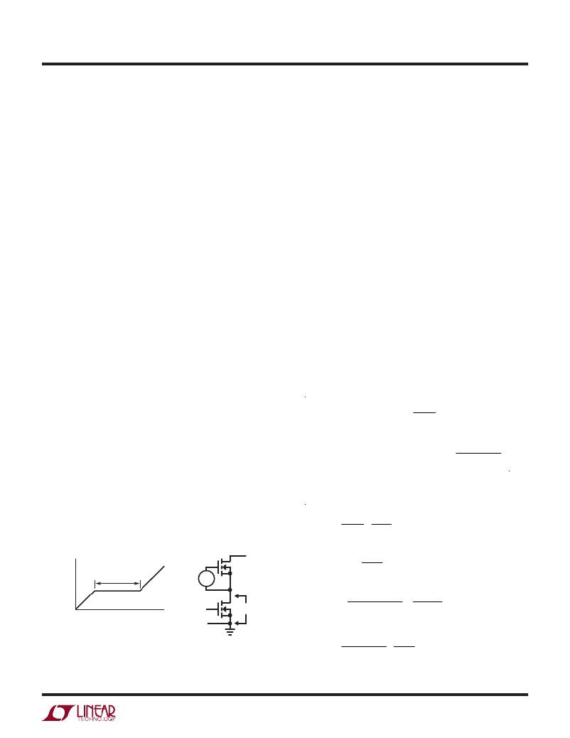
�MOSFET� input� capacitance� is� a� combination� of� sev-�
�eral� components� but� can� be� taken� from� the� typical� “gate�
�charge”� curve� included� on� most� data� sheets� (Figure� 5).�
�The� curve� is� generated� by� forcing� a� constant� input� cur-�
�rent� into� the� gate� of� a� common� source,� current� source�
�loaded� stage� and� then� plotting� the� gate� voltage� versus�
�time.� The� initial� slope� is� the� effect� of� the� gate-to-source�
�and� the� gate-to-drain� capacitance.� The� flat� portion� of� the�
�curve� is� the� result� of� the� Miller� multiplication� effect� of� the�
�drain-to-gate� capacitance� as� the� drain� drops� the� voltage�
�across� the� current� source� load.� The� upper� sloping� line� is�
�due� to� the� drain-to-gate� accumulation� capacitance� and�
�the� gate-to-source� capacitance.� The� Miller� charge� (the�
�increase� in� coulombs� on� the� horizontal� axis� from� a� to� b�
�while� the� curve� is� flat)� is� specified� for� a� given� V� DS� drain�
�voltage,� but� can� be� adjusted� for� different� V� DS� voltages� by�
�multiplying� by� the� ratio� of� the� application� V� DS� to� the� curve�
�specified� V� DS� values.� A� way� to� estimate� the� C� MILLER� term�
�is� to� take� the� change� in� gate� charge� from� points� a� and� b�
�on� a� manufacturer’s� data� sheet� and� divide� by� the� stated�
�V� DS� voltage� specified.� C� MILLER� is� the� most� important� se-�
�lection� criteria� for� determining� the� transition� loss� term� in�
�the� top� MOSFET� but� is� not� directly� specified� on� MOSFET�
�data� sheets.� C� RSS� and� C� OS� are� specified� sometimes� but�
�definitions� of� these� parameters� are� not� included.�
�When� the� controller� is� operating� in� continuous� mode� the�
�duty� cycles� for� the� top� and� bottom� MOSFETs� are� given� by:�
�Main� Switch� Duty� Cycle� =�
�?� V – V� OUT� ?�
�?�
�?� V� IN� ?�
�The� power� dissipation� for� the� main� and� synchronous�
�MOSFETs� at� maximum� output� current� are� given� by:�
�2�
�V� IN� ?� N� ?�
�V�
�(� R� DR� )� (� C� MILLER� )� ?�
�V� IN2�
�?� (� f� )�
�?� ?� V� CC� –� V� TH(IL)�
�V� TH(IL)� ?� ?�
�V� –� V� OUT� ?� I� MAX� ?�
�P� SYNC� =� IN� (� 1� +� δ� )� R� DS(ON)�
�V� GS�
�MILLER� EFFECT�
�a� b�
�+�
�Q� IN� V� GS�
�C� MILLER� =� (Q� B� –� Q� A� )/V� DS� –�
�Figure� 5.� Gate� Charge� Characteristic�
�V� IN�
�+� V� DS�
�–�
�3731� F05�
�?� 1� 1� ?�
�I� MAX�
�2N�
�?� +�
�?� ?�
�V� IN� ?� N� ?�
�2�
�3731fc�
�15�
�相关PDF资料 |
PDF描述 |
|---|---|
| VI-J5J-EW-F4 | CONVERTER MOD DC/DC 36V 100W |
| VI-J5J-EW-F2 | CONVERTER MOD DC/DC 36V 100W |
| LTC3736EGN-1 | IC REG CTRLR BUCK PWM CM 24-SSOP |
| VI-J5J-EW-F1 | CONVERTER MOD DC/DC 36V 100W |
| VI-J54-EW-F4 | CONVERTER MOD DC/DC 48V 100W |
相关代理商/技术参数 |
参数描述 |
|---|---|
| LTC3731CUH | 功能描述:IC REG CTRLR BUCK PWM CM 32-QFN RoHS:否 类别:集成电路 (IC) >> PMIC - 稳压器 - DC DC 切换控制器 系列:PolyPhase® 标准包装:4,500 系列:PowerWise® PWM 型:控制器 输出数:1 频率 - 最大:1MHz 占空比:95% 电源电压:2.8 V ~ 5.5 V 降压:是 升压:无 回扫:无 反相:无 倍增器:无 除法器:无 Cuk:无 隔离:无 工作温度:-40°C ~ 125°C 封装/外壳:6-WDFN 裸露焊盘 包装:带卷 (TR) 配用:LM1771EVAL-ND - BOARD EVALUATION LM1771 其它名称:LM1771SSDX |
| LTC3731CUH#PBF | 功能描述:IC REG CTRLR BUCK PWM CM 32-QFN RoHS:是 类别:集成电路 (IC) >> PMIC - 稳压器 - DC DC 切换控制器 系列:PolyPhase® 标准包装:4,500 系列:PowerWise® PWM 型:控制器 输出数:1 频率 - 最大:1MHz 占空比:95% 电源电压:2.8 V ~ 5.5 V 降压:是 升压:无 回扫:无 反相:无 倍增器:无 除法器:无 Cuk:无 隔离:无 工作温度:-40°C ~ 125°C 封装/外壳:6-WDFN 裸露焊盘 包装:带卷 (TR) 配用:LM1771EVAL-ND - BOARD EVALUATION LM1771 其它名称:LM1771SSDX |
| LTC3731CUH#PBF | 制造商:Linear Technology 功能描述:DC-DC CONVERTER, BUCK, 600KHZ, 240A, QFN |
| LTC3731CUH#TR | 功能描述:IC REG CTRLR BUCK PWM CM 32-QFN RoHS:否 类别:集成电路 (IC) >> PMIC - 稳压器 - DC DC 切换控制器 系列:PolyPhase® 标准包装:4,500 系列:PowerWise® PWM 型:控制器 输出数:1 频率 - 最大:1MHz 占空比:95% 电源电压:2.8 V ~ 5.5 V 降压:是 升压:无 回扫:无 反相:无 倍增器:无 除法器:无 Cuk:无 隔离:无 工作温度:-40°C ~ 125°C 封装/外壳:6-WDFN 裸露焊盘 包装:带卷 (TR) 配用:LM1771EVAL-ND - BOARD EVALUATION LM1771 其它名称:LM1771SSDX |
| LTC3731CUH#TRPBF | 功能描述:IC REG CTRLR BUCK PWM CM 32-QFN RoHS:是 类别:集成电路 (IC) >> PMIC - 稳压器 - DC DC 切换控制器 系列:PolyPhase® 标准包装:4,500 系列:PowerWise® PWM 型:控制器 输出数:1 频率 - 最大:1MHz 占空比:95% 电源电压:2.8 V ~ 5.5 V 降压:是 升压:无 回扫:无 反相:无 倍增器:无 除法器:无 Cuk:无 隔离:无 工作温度:-40°C ~ 125°C 封装/外壳:6-WDFN 裸露焊盘 包装:带卷 (TR) 配用:LM1771EVAL-ND - BOARD EVALUATION LM1771 其它名称:LM1771SSDX |
发布紧急采购,3分钟左右您将得到回复。