- 您现在的位置:买卖IC网 > PDF目录369885 > LXT386LE PCM TRANSCEIVER|QUAD|CEPT PCM-30/E-1|CMOS|QFP|100PIN|PLASTIC PDF资料下载
参数资料
| 型号: | LXT386LE |
| 英文描述: | PCM TRANSCEIVER|QUAD|CEPT PCM-30/E-1|CMOS|QFP|100PIN|PLASTIC |
| 中文描述: | 的PCM收发器|四|优税PCM-30/E-1 |的CMOS | QFP封装| 100引脚|塑料 |
| 文件页数: | 13/80页 |
| 文件大小: | 1112K |
| 代理商: | LXT386LE |
第1页第2页第3页第4页第5页第6页第7页第8页第9页第10页第11页第12页当前第13页第14页第15页第16页第17页第18页第19页第20页第21页第22页第23页第24页第25页第26页第27页第28页第29页第30页第31页第32页第33页第34页第35页第36页第37页第38页第39页第40页第41页第42页第43页第44页第45页第46页第47页第48页第49页第50页第51页第52页第53页第54页第55页第56页第57页第58页第59页第60页第61页第62页第63页第64页第65页第66页第67页第68页第69页第70页第71页第72页第73页第74页第75页第76页第77页第78页第79页第80页
Octal T1/E1/J1 Transceiver
—
LXT384
Datasheet
13
7
7
8
8
D3
D3
D2
D2
TNEG6
UBS6
TPOS6
TDATA6
DI
DI
DI
DI
Transmit Negative Data Input.
Unipolar/Bipolar Select Input.
Transmit Positive Data Input.
Transmit Data Input.
Bipolar Mode:
TPOS/TNEG are active High NRZ inputs. TPOS indicates the
transmission of a positive pulse whereas TNEG indicates the
transmission of a negative pulse.
Unipolar Mode:
When TNEG/UBS is pulled High for more than 16 consecutive TCLK
clock cycles, unipolar I/O is selected. In unipolar mode, B8ZS/HDB3 or
AMI encoding/decoding is determined by the CODEN pin (hardware
mode) or by the CODEN bit in the GCR register (software mode).
TDATA is the data input in unipolar I/O mode.
9
D1
TCLK6
DI
Transmit Clock Input.
10
E1
MCLK
DI
Master Clock Input. MCLK is an independent, free-running reference
clock. It
’
s frequency should be 1.544 MHz for T1 operation and 2.048
MHz for E1 operation.
This reference clock is used to generate several internal reference
signals:
Timing reference for the integrated clock recovery unit
Timing reference for the integrated digital jitter attenuator
Generation of RCLK signal during a loss of signal condition
Reference clock during a blue alarm transmit all ones condition
Reference timing for the parallel processor wait state generation
logic
If MCLK is High, the PLL clock recovery circuit is disabled. In this mode,
the LXT384 operates as simple data receiver.
If MCLK is Low, the complete receive path is powered down and the
output pins RCLK, RPOS and RNEG are switched to tri-state mode.
MCLK is not required if LXT384 is used as a simple analog front-end
without clock recovery and jitter attenuation.
Note:
Wait state generation via RDY/ACK is not available if MCLK is
not provided.
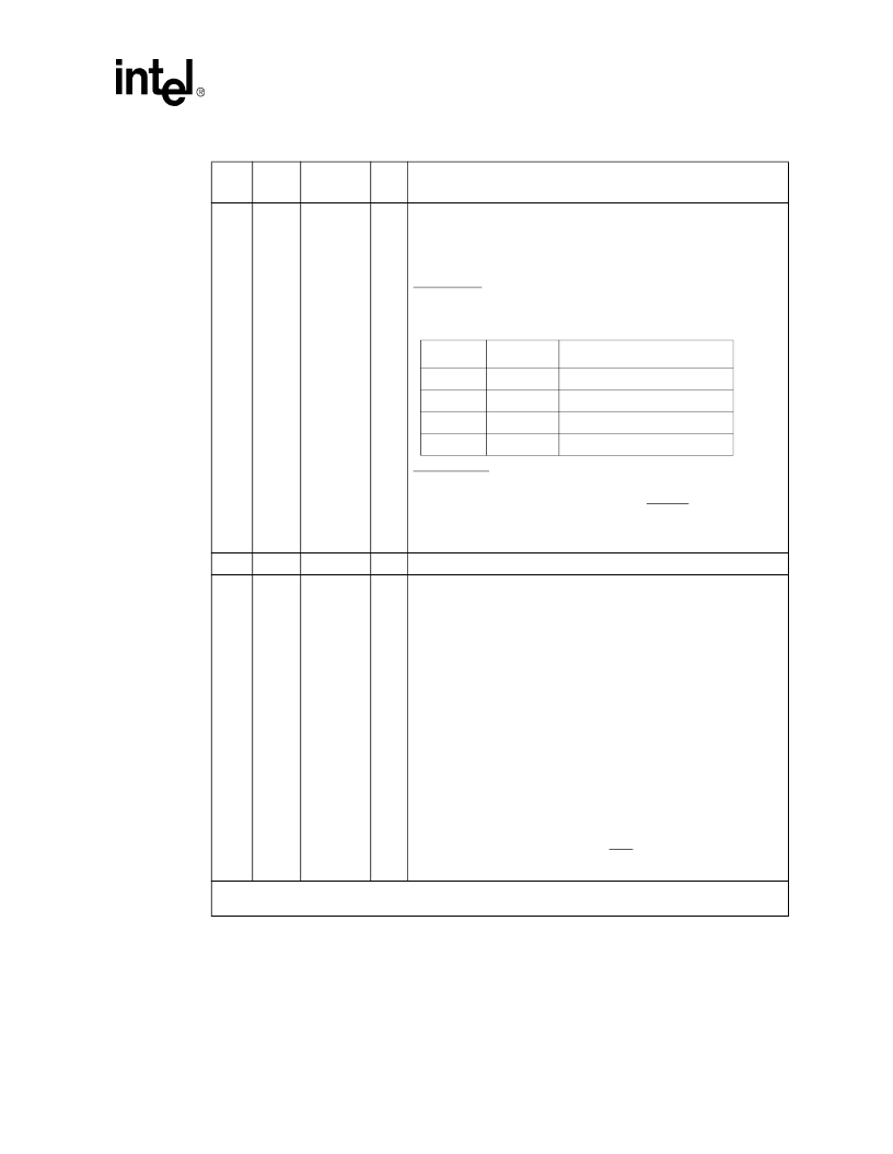
Table 1. LXT384 Pin Description (Sheet 3 of 12)
Pin #
QFP
Ball #
PBGA
Symbol
I/O
1
Description
1. DI: Digital Input; DO: Digital Output; DI/O: Digital Bidirectional Port; AI: Analog Input; AO: Analog Output
S: Power Supply; N.C.: Not Connected.
TPOS
TNEG
Selection
0
0
Space
1
0
Positive Mark
0
1
Negative Mark
1
1
Space
相关PDF资料 |
PDF描述 |
|---|---|
| LXT388LE | PCM TRANSCEIVER|DUAL|CEPT PCM-30/E-1|CMOS|QFP|100PIN|PLASTIC |
| LXT400JE | Hermetically Sealed, 3.3V, High Speed, High CMR, Logic Gate Optocoupler |
| LXT6155LE | Telecomm/Datacomm |
| LXT6251A | ATM/SONET MAPPER|CMOS|QFP|208PIN|PLASTIC |
| LXT903PC | LAN Transceiver |
相关代理商/技术参数 |
参数描述 |
|---|---|
| LXT388LE | 制造商:未知厂家 制造商全称:未知厂家 功能描述:PCM TRANSCEIVER|DUAL|CEPT PCM-30/E-1|CMOS|QFP|100PIN|PLASTIC |
| LXT400 | 制造商:LVL1 制造商全称:LVL1 功能描述:All Rate Extended Range Switched 56/DDS Transceiver |
| LXT400JE | 制造商:未知厂家 制造商全称:未知厂家 功能描述:Transceiver Circuit For Telecommunications |
| LXT441 | 制造商:LVL1 制造商全称:LVL1 功能描述:Switched 56/DDS Integrated DSU/CSU |
| LXT6155 | 制造商:INTEL 制造商全称:Intel Corporation 功能描述:155 Mbps SDH/SONET/ATM Transceiver |
发布紧急采购,3分钟左右您将得到回复。