- 您现在的位置:买卖IC网 > PDF目录369885 > LXT386LE PCM TRANSCEIVER|QUAD|CEPT PCM-30/E-1|CMOS|QFP|100PIN|PLASTIC PDF资料下载
参数资料
| 型号: | LXT386LE |
| 英文描述: | PCM TRANSCEIVER|QUAD|CEPT PCM-30/E-1|CMOS|QFP|100PIN|PLASTIC |
| 中文描述: | 的PCM收发器|四|优税PCM-30/E-1 |的CMOS | QFP封装| 100引脚|塑料 |
| 文件页数: | 22/80页 |
| 文件大小: | 1112K |
| 代理商: | LXT386LE |
第1页第2页第3页第4页第5页第6页第7页第8页第9页第10页第11页第12页第13页第14页第15页第16页第17页第18页第19页第20页第21页当前第22页第23页第24页第25页第26页第27页第28页第29页第30页第31页第32页第33页第34页第35页第36页第37页第38页第39页第40页第41页第42页第43页第44页第45页第46页第47页第48页第49页第50页第51页第52页第53页第54页第55页第56页第57页第58页第59页第60页第61页第62页第63页第64页第65页第66页第67页第68页第69页第70页第71页第72页第73页第74页第75页第76页第77页第78页第79页第80页
LXT384
—
Octal T1/E1/J1 Transceiver
22
Datasheet
2.0
Functional Description
Figure 1 is a block diagram of the LXT384. The LXT384 is a fully integrated octal line interface
unit designed for T1 1.544 Mbps and E1 2.048 Mbps short haul applications.
Each transceiver front end interfaces with four lines, one pair for transmit, one pair for receive.
These two lines comprise a digital data loop for full duplex transmission.
The LXT384 can be controlled through hard-wired pins or by a microprocessor through a serial or
parallel interface (Host mode).
The transmitter timing reference is TCLK, and the receiver reference clock is MCLK. The LXT384
is designed to operate without any reference clock when used as an analog front-end (line driver
and data recovery). MCLK is mandatory if the on chip clock recovery capability is used. All eight
clock recovery circuits share the same reference clock defined by the MCLK input signal.
2.1
Initialization
During power up, the transceiver remains static until the power supply reaches approximately 60%
of VCC. During power-up, an internal reset sets all registers to their default values and resets the
status and state machines for the LOS.
129
130
D5
C5
TTIP6
TRING6
AO
AO
Transmit Tip Output.
Transmit Ring Output.
131
C6, D6
TGND6
S
Transmit Driver Ground.
132
133
C7
D7
RTIP6
RRING6
AI
AI
Receive Tip Input.
Receive Ring Input.
134
A6, B6
TGND7
S
Transmit Driver Ground.
135
136
A5
B5
TRING7
TTIP7
AO
AO
Transmit Ring Output.
Transmit Tip Output.
137
A4, B4
TVCC7
S
Transmit Driver Power Supply.
138
139
B7
A7
RRING7
RTIP7
AI
AI
Receive Ring Input.
Receive Tip Input.
140
E4
LOS7
DO
Loss of Signal Output.
141
141
142
142
A3
A3
A2
A2
RNEG7
BPV7
RPOS7
RDATA7
DO
DO
DO
DO
Receive Negative Data Output.
Bipolar Violation Detect Output.
Receive Positive Data Output.
Receive Data Output.
143
A1
RCLK7
DO
Receive Clock Output.
144
144
B3
B3
TNEG7
UBS7
DI
DI
Transmit Negative Data Input.
Unipolar/Bipolar Select Input.
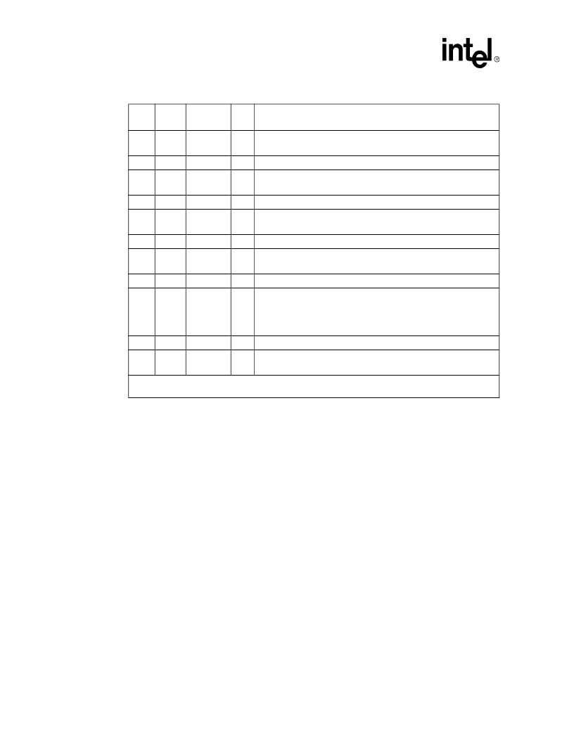
Table 1. LXT384 Pin Description (Sheet 12 of 12)
Pin #
QFP
Ball #
PBGA
Symbol
I/O
1
Description
1. DI: Digital Input; DO: Digital Output; DI/O: Digital Bidirectional Port; AI: Analog Input; AO: Analog Output
S: Power Supply; N.C.: Not Connected.
相关PDF资料 |
PDF描述 |
|---|---|
| LXT388LE | PCM TRANSCEIVER|DUAL|CEPT PCM-30/E-1|CMOS|QFP|100PIN|PLASTIC |
| LXT400JE | Hermetically Sealed, 3.3V, High Speed, High CMR, Logic Gate Optocoupler |
| LXT6155LE | Telecomm/Datacomm |
| LXT6251A | ATM/SONET MAPPER|CMOS|QFP|208PIN|PLASTIC |
| LXT903PC | LAN Transceiver |
相关代理商/技术参数 |
参数描述 |
|---|---|
| LXT388LE | 制造商:未知厂家 制造商全称:未知厂家 功能描述:PCM TRANSCEIVER|DUAL|CEPT PCM-30/E-1|CMOS|QFP|100PIN|PLASTIC |
| LXT400 | 制造商:LVL1 制造商全称:LVL1 功能描述:All Rate Extended Range Switched 56/DDS Transceiver |
| LXT400JE | 制造商:未知厂家 制造商全称:未知厂家 功能描述:Transceiver Circuit For Telecommunications |
| LXT441 | 制造商:LVL1 制造商全称:LVL1 功能描述:Switched 56/DDS Integrated DSU/CSU |
| LXT6155 | 制造商:INTEL 制造商全称:Intel Corporation 功能描述:155 Mbps SDH/SONET/ATM Transceiver |
发布紧急采购,3分钟左右您将得到回复。