- 您现在的位置:买卖IC网 > PDF目录369885 > LXT388LE PCM TRANSCEIVER|DUAL|CEPT PCM-30/E-1|CMOS|QFP|100PIN|PLASTIC PDF资料下载
参数资料
| 型号: | LXT388LE |
| 英文描述: | PCM TRANSCEIVER|DUAL|CEPT PCM-30/E-1|CMOS|QFP|100PIN|PLASTIC |
| 中文描述: | 的PCM收发器|双|优税PCM-30/E-1 |的CMOS | QFP封装| 100引脚|塑料 |
| 文件页数: | 12/80页 |
| 文件大小: | 1112K |
| 代理商: | LXT388LE |
第1页第2页第3页第4页第5页第6页第7页第8页第9页第10页第11页当前第12页第13页第14页第15页第16页第17页第18页第19页第20页第21页第22页第23页第24页第25页第26页第27页第28页第29页第30页第31页第32页第33页第34页第35页第36页第37页第38页第39页第40页第41页第42页第43页第44页第45页第46页第47页第48页第49页第50页第51页第52页第53页第54页第55页第56页第57页第58页第59页第60页第61页第62页第63页第64页第65页第66页第67页第68页第69页第70页第71页第72页第73页第74页第75页第76页第77页第78页第79页第80页
LXT384
—
Octal T1/E1/J1 Transceiver
12
Datasheet
4
4
5
5
C3
C3
C2
C2
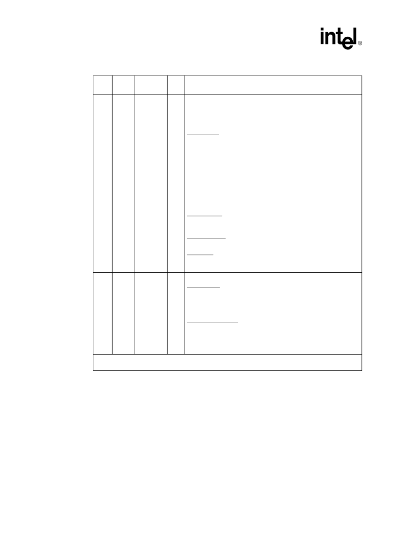
RNEG6
BPV6
RPOS6
RDATA6
DO
DO
DO
DO
Receive Negative Data Output.
Bipolar Violation Detect Output.
Receive Positive Data Output.
Receive Data Output
Bipolar Mode:
In clock recovery mode, these pins act as active High bipolar non return
to zero (NRZ) receive signal outputs. A High signal on RPOS
corresponds to receipt of a positive pulse on RTIP/RRING. A High
signal on RNEG corresponds to receipt of a negative pulse on RTIP/
RRING. These signals are valid on the falling or rising edges of RCLK
depending on the CLKE input.
In Data recovery mode, these pins act as RZ data receiver outputs. The
output polarity is selectable with CLKE (Active High output polarity when
CLKE is High and Active Low Polarity when CLKE is Low).
RPOS and RNEG will go to the high impedance state when the MCLK
pin is Low.
Unipolar Mode:
In uni-polar mode, the LXT384 asserts BPV High if any in-service Line
Code Violation is detected. RDATA acts as the receive data output.
Hardware Mode:
During a LOS condition, RPOS and RNEG will remain active.
Host Mode:
RPOS and RNEG will either remain active or insert AIS into the receive
path. Selection is determined by the RAISEN bit in the GCR register.
6
C1
RCLK6
DO
Receive Clock Output.
Normal Mode:
This pin provides the recovered clock from the signal received at RTIP
and RRING. Under LOS conditions there is a transition from RCLK
signal (derived from the recovered data) to MCLK signal at the RCLK
output.
Data Recovery Mode:
If MCLK is High, the clock recovery circuit is disabled and RPOS and
RNEG are internally connected to an EXOR that is fed to the RCLK
output for external clock recovery applications.
RCLK will be in high impedance state if the MCLK pin is Low.
Table 1. LXT384 Pin Description (Sheet 2 of 12)
Pin #
QFP
Ball #
PBGA
Symbol
I/O
1
Description
1. DI: Digital Input; DO: Digital Output; DI/O: Digital Bidirectional Port; AI: Analog Input; AO: Analog Output
S: Power Supply; N.C.: Not Connected.
相关PDF资料 |
PDF描述 |
|---|---|
| LXT400JE | Hermetically Sealed, 3.3V, High Speed, High CMR, Logic Gate Optocoupler |
| LXT6155LE | Telecomm/Datacomm |
| LXT6251A | ATM/SONET MAPPER|CMOS|QFP|208PIN|PLASTIC |
| LXT903PC | LAN Transceiver |
| LXT905LC | Laser Mouse VCSEL Assembly Clip |
相关代理商/技术参数 |
参数描述 |
|---|---|
| LXT400 | 制造商:LVL1 制造商全称:LVL1 功能描述:All Rate Extended Range Switched 56/DDS Transceiver |
| LXT400JE | 制造商:未知厂家 制造商全称:未知厂家 功能描述:Transceiver Circuit For Telecommunications |
| LXT441 | 制造商:LVL1 制造商全称:LVL1 功能描述:Switched 56/DDS Integrated DSU/CSU |
| LXT6155 | 制造商:INTEL 制造商全称:Intel Corporation 功能描述:155 Mbps SDH/SONET/ATM Transceiver |
| LXT6155LE | 制造商:未知厂家 制造商全称:未知厂家 功能描述:Telecomm/Datacomm |
发布紧急采购,3分钟左右您将得到回复。