- 您现在的位置:买卖IC网 > PDF目录299432 > M28W640ECT70ZB1E (STMICROELECTRONICS) 4M X 16 FLASH 3V PROM, 70 ns, PBGA48 PDF资料下载
参数资料
| 型号: | M28W640ECT70ZB1E |
| 厂商: | STMICROELECTRONICS |
| 元件分类: | PROM |
| 英文描述: | 4M X 16 FLASH 3V PROM, 70 ns, PBGA48 |
| 封装: | 6.39 X 10.50 MM, 0.75 MM PITCH, LEAD FREE, TFBGA-48 |
| 文件页数: | 3/54页 |
| 文件大小: | 957K |
| 代理商: | M28W640ECT70ZB1E |
第1页第2页当前第3页第4页第5页第6页第7页第8页第9页第10页第11页第12页第13页第14页第15页第16页第17页第18页第19页第20页第21页第22页第23页第24页第25页第26页第27页第28页第29页第30页第31页第32页第33页第34页第35页第36页第37页第38页第39页第40页第41页第42页第43页第44页第45页第46页第47页第48页第49页第50页第51页第52页第53页第54页
11/54
M28W640ECT, M28W640ECB
COMMAND INTERFACE
All Bus Write operations to the memory are inter-
preted by the Command Interface. Commands
consist of one or more sequential Bus Write oper-
ations. An internal Program/Erase Controller han-
dles all timings and verifies the correct execution
of the Program and Erase commands. The Pro-
gram/Erase Controller provides a Status Register
whose output may be read at any time during, to
monitor the progress of the operation, or the Pro-
gram/Erase states. See Table 3, Command
Codes, for a summary of the commands and see
rent/Next, for a summary of the Command Inter-
face.
The Command Interface is reset to Read mode
when power is first applied, when exiting from Re-
set or whenever VDD is lower than VLKO. Com-
mand sequences must be followed exactly. Any
invalid combination of commands will reset the de-
vice to Read mode. Refer to Table 4, Commands,
in conjunction with the text descriptions below.
Read Memory Array Command
The Read command returns the memory to its
Read mode. One Bus Write cycle is required to is-
sue the Read Memory Array command and return
the memory to Read mode. Subsequent read op-
erations will read the addressed location and out-
put the data. When a device Reset occurs, the
memory defaults to Read mode.
Read Status Register Command
The Status Register indicates when a program or
erase operation is complete and the success or
failure of the operation itself. Issue a Read Status
Register command to read the Status Register’s
contents. Subsequent Bus Read operations read
the Status Register at any address, until another
command is issued. See Table 11, Status Register
Bits, for details on the definitions of the bits.
The Read Status Register command may be is-
sued at any time, even during a Program/Erase
operation. Any Read attempt during a Program/
Erase operation will automatically output the con-
tent of the Status Register.
Read Electronic Signature Command
The Read Electronic Signature command reads
the Manufacturer and Device Codes and the Block
Locking Status, or the Protection Register.
The Read Electronic Signature command consists
of one write cycle, a subsequent read will output
the Manufacturer Code, the Device Code, the
Block Lock and Lock-Down Status, or the Protec-
the valid address.
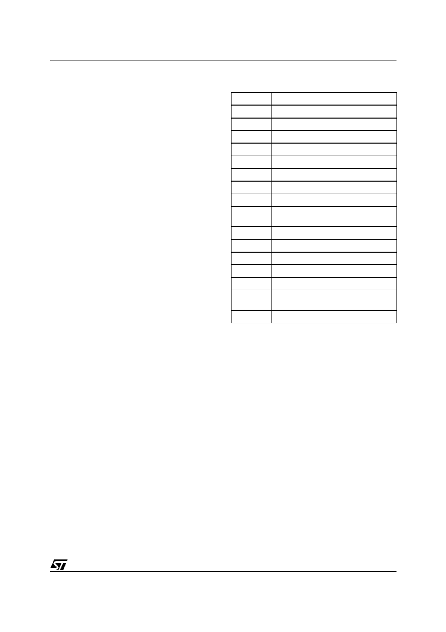
Table 3. Command Codes
Read CFI Query Command
The Read Query Command is used to read data
from the Common Flash Interface (CFI) Memory
Area, allowing programming equipment or appli-
cations to automatically match their interface to
the characteristics of the device. One Bus Write
cycle is required to issue the Read Query Com-
mand. Once the command is issued subsequent
Bus Read operations read from the Common
Flash Interface Memory Area. See Appendix B,
in the Common Flash Interface memory area.
Block Erase Command
The Block Erase command can be used to erase
a block. It sets all the bits within the selected block
to ’1’. All previous data in the block is lost. If the
block is protected then the Erase operation will
abort, the data in the block will not be changed and
the Status Register will output the error.
Two Bus Write cycles are required to issue the
command.
■
The first bus cycle sets up the Erase
command.
Hex Code
Command
01h
Block Lock confirm
10h
Program
20h
Erase
2Fh
Block Lock-Down confirm
30h
Double Word Program
40h
Program
50h
Clear Status Register
56h
Quadruple Word Program
60h
Block Lock, Block Unlock, Block Lock-
Down
70h
Read Status Register
90h
Read Electronic Signature
98h
Read CFI Query
B0h
Program/Erase Suspend
C0h
Protection Register Program
D0h
Program/Erase Resume, Block Unlock
confirm
FFh
Read Memory Array
相关PDF资料 |
PDF描述 |
|---|---|
| M28W640ECT85N1E | 4M X 16 FLASH 3V PROM, 85 ns, PDSO48 |
| M29W040B70N1E | 4 Mbit 512Kb x8, Uniform Block Low Voltage Single Supply Flash Memory |
| M29W040B70N1F | 4 Mbit 512Kb x8, Uniform Block Low Voltage Single Supply Flash Memory |
| M29W040B70N6E | 4 Mbit 512Kb x8, Uniform Block Low Voltage Single Supply Flash Memory |
| M29W040B70N6F | 4 Mbit 512Kb x8, Uniform Block Low Voltage Single Supply Flash Memory |
相关代理商/技术参数 |
参数描述 |
|---|---|
| M28W640ECT70ZB6 | 功能描述:闪存 64M (4Mx16) 70ns RoHS:否 制造商:ON Semiconductor 数据总线宽度:1 bit 存储类型:Flash 存储容量:2 MB 结构:256 K x 8 定时类型: 接口类型:SPI 访问时间: 电源电压-最大:3.6 V 电源电压-最小:2.3 V 最大工作电流:15 mA 工作温度:- 40 C to + 85 C 安装风格:SMD/SMT 封装 / 箱体: 封装:Reel |
| M28W640ECT70ZB6T | 功能描述:闪存 64M (4Mx16) 70ns RoHS:否 制造商:ON Semiconductor 数据总线宽度:1 bit 存储类型:Flash 存储容量:2 MB 结构:256 K x 8 定时类型: 接口类型:SPI 访问时间: 电源电压-最大:3.6 V 电源电压-最小:2.3 V 最大工作电流:15 mA 工作温度:- 40 C to + 85 C 安装风格:SMD/SMT 封装 / 箱体: 封装:Reel |
| M28W640FCB70N6 | 制造商:STMicroelectronics 功能描述: |
| M28W640FCB70N6E | 功能描述:闪存 STD FLASH 64 MEG RoHS:否 制造商:ON Semiconductor 数据总线宽度:1 bit 存储类型:Flash 存储容量:2 MB 结构:256 K x 8 定时类型: 接口类型:SPI 访问时间: 电源电压-最大:3.6 V 电源电压-最小:2.3 V 最大工作电流:15 mA 工作温度:- 40 C to + 85 C 安装风格:SMD/SMT 封装 / 箱体: 封装:Reel |
| M28W640FCB70N6F | 功能描述:闪存 STD FLASH 64 MEG RoHS:否 制造商:ON Semiconductor 数据总线宽度:1 bit 存储类型:Flash 存储容量:2 MB 结构:256 K x 8 定时类型: 接口类型:SPI 访问时间: 电源电压-最大:3.6 V 电源电压-最小:2.3 V 最大工作电流:15 mA 工作温度:- 40 C to + 85 C 安装风格:SMD/SMT 封装 / 箱体: 封装:Reel |
发布紧急采购,3分钟左右您将得到回复。