- 您现在的位置:买卖IC网 > PDF目录80464 > M38039GCHWG 8-BIT, MROM, 8.4 MHz, MICROCONTROLLER, PBGA64 PDF资料下载
参数资料
| 型号: | M38039GCHWG |
| 元件分类: | 微控制器/微处理器 |
| 英文描述: | 8-BIT, MROM, 8.4 MHz, MICROCONTROLLER, PBGA64 |
| 封装: | 6 X 6 MM, 0.65 PITCH, FLGA-64 |
| 文件页数: | 46/103页 |
| 文件大小: | 1412K |
| 代理商: | M38039GCHWG |
第1页第2页第3页第4页第5页第6页第7页第8页第9页第10页第11页第12页第13页第14页第15页第16页第17页第18页第19页第20页第21页第22页第23页第24页第25页第26页第27页第28页第29页第30页第31页第32页第33页第34页第35页第36页第37页第38页第39页第40页第41页第42页第43页第44页第45页当前第46页第47页第48页第49页第50页第51页第52页第53页第54页第55页第56页第57页第58页第59页第60页第61页第62页第63页第64页第65页第66页第67页第68页第69页第70页第71页第72页第73页第74页第75页第76页第77页第78页第79页第80页第81页第82页第83页第84页第85页第86页第87页第88页第89页第90页第91页第92页第93页第94页第95页第96页第97页第98页第99页第100页第101页第102页第103页
REJ03B0166-0113 Rev.1.13
Aug 21, 2009
Page 47 of 100
3803 Group (Spec.H QzROM version)
(2) Asynchronous Serial I/O (UART) Mode
Clock asynchronous serial I/O mode (UART) can be selected by
clearing the serial I/O1 mode selection bit (b6) of the serial I/O1
control register to “0”.
Eight serial data transfer formats can be selected, and the transfer
formats used by a transmitter and receiver must be identical.
The transmit and receive shift registers each have the buffer
register 1, but the two buffer registers have the same address in a
memory. Since the shift register cannot be written to or read from
directly, transmit data is written to the transmit buffer register 1,
and receive data is read from the receive buffer register 1.
The transmit buffer register 1 can also hold the next data to be
transmitted, and the receive buffer register 1 can hold a character
while the next character is being received.
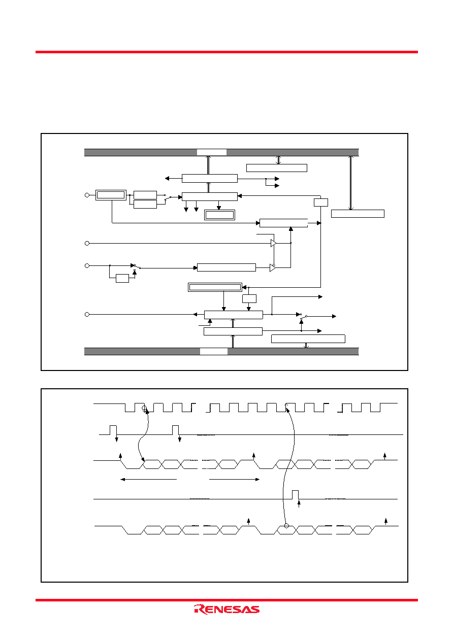
Fig 38. Block diagram of UART serial I/O1
Fig 39. Operation of UART serial I/O1
f(XIN)
1/4
OE
PE FE
1/16
Data bus
Receive buffer register 1
Address 001816
Receive shift register 1
Receive buffer full flag (RBF)
Receive interrupt request (RI)
Baud rate generator
Frequency division ratio 1/(n+1)
Address 001C16
ST/SP/PA generator
Transmit buffer register 1
Transmit shift register 1
Address 001816
Transmit shift
completion flag (TSC)
Transmit buffer empty flag (TBE)
Transmit interrupt request (TI)
Address 001916
ST detector
SP detector
UART1 control register
Address 001B16
Character length selection bit
Address 001A16
BRG count source selection bit
Transmit interrupt source selection bit
Serial I/O1 synchronous clock selection bit
Clock control circuit
Character length selection bit
7 bits
8 bits
Serial I/O1 status register
Serial I/O1 control register
P46/SCLK1
P44/RXD1
P45/TXD1
(f(XCIN) in low-speed mode)
TSC=0
TBE=1
RBF=0
TBE=0
RBF=1
TBE=1
TSC=1*
ST
D0
D1
SP
D0
D1
ST
SP
Transmit or
receive clock
Transmit buffer register 1
write signal
Serial output
TXD1
Receive buffer register 1
read signal
Serial input RXD1
Generated at 2nd bit in 2-stop-bit mode
1 start bit
7 or 8 data bit
1 or 0 parity bit
1 or 2 stop bit (s)
Notes 1: Error flag detection occurs at the same time that the RBF flag becomes “1” (at 1st stop bit, during reception).
2: As the transmit interrupt (TI), when either the TBE or TSC flag becomes “1”, can be selected to occur depending on the setting of the transmit interrupt source
selection bit (TIC) of the serial I/O1 control register.
3: The receive interrupt (RI) is set when the RBF flag becomes “1”.
4: After data is written to the transmit buffer when TSC=1, 0.5 to 1.5 cycles of the data shift cycle are necessary until changing to TSC=0.
ST
D0
D1
SP
D0
D1
ST
SP
相关PDF资料 |
PDF描述 |
|---|---|
| MSP430F2350IYFF | 16-BIT, FLASH, 16 MHz, RISC MICROCONTROLLER, PBGA49 |
| MK1707D | 108 MHz, OTHER CLOCK GENERATOR, PDSO8 |
| MPC8347ZUAGFA | 32-BIT, 400 MHz, MICROPROCESSOR, PBGA672 |
| M30302GGPGP | 16-BIT, OTPROM, 16 MHz, MICROCONTROLLER, PQFP100 |
| MC3S12HN64J3CAA | 16-BIT, MROM, 25 MHz, MICROCONTROLLER, PQFP80 |
相关代理商/技术参数 |
参数描述 |
|---|---|
| M38049FFFP#U0 | 制造商:Renesas Electronics Corporation 功能描述: |
| M38049FFLHP#U0 | 制造商:Renesas Electronics Corporation 功能描述: |
| M38049RLSS | 功能描述:DEV EMULATOR CHIP RAM 2KB 64SDIP RoHS:否 类别:编程器,开发系统 >> 内电路编程器、仿真器以及调试器 系列:- 产品变化通告:Development Systems Discontinuation 19/Jul/2010 标准包装:1 系列:* 类型:* 适用于相关产品:* 所含物品:* |
| M3806 | 功能描述:电缆固定件和配件 LTSCG 625 BLACK RoHS:否 制造商:Heyco 类型:Cable Grips, Liquid Tight 材料:Nylon 颜色:Black 安装方法:Cable 最大光束直径:11.4 mm 抗拉强度: |
| M3806 BK001 | 制造商:Alpha Wire Company 功能描述:CBL 8COND 18AWG BLK 1000' |
发布紧急采购,3分钟左右您将得到回复。