- 您现在的位置:买卖IC网 > PDF目录383305 > M5M5Y5672TG-20 (Mitsubishi Electric Corporation) 18874368-BIT(262144-WORD BY 72-BIT) NETWORK SRAM PDF资料下载
参数资料
| 型号: | M5M5Y5672TG-20 |
| 厂商: | Mitsubishi Electric Corporation |
| 英文描述: | 18874368-BIT(262144-WORD BY 72-BIT) NETWORK SRAM |
| 中文描述: | 18874368位(262144 - Word的72位)网络的SRAM |
| 文件页数: | 4/27页 |
| 文件大小: | 240K |
| 代理商: | M5M5Y5672TG-20 |
第1页第2页第3页当前第4页第5页第6页第7页第8页第9页第10页第11页第12页第13页第14页第15页第16页第17页第18页第19页第20页第21页第22页第23页第24页第25页第26页第27页
MITSUBISHI LSIs
M5M5Y5672TG – 25,22,20
18874368-BIT(262144-WORD BY 72-BIT) NETWORK SRAM
4
MITSUBISHI
ELECTRIC
Advanced Information
M5M5Y5672TG REV.0.1
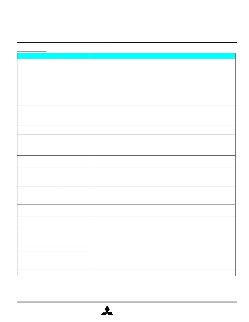
PIN FUNCTION
Pin
Name
Function
A0~A17
Synchronous
Address
Inputs
These inputs are registered and must meet the setup and hold times around the rising edge of
CLK. A0 and A1 are the two least significant bits (LSB) of the address field and set the internal
burst counter if burst is desired.
These active LOW inputs allow individual bytes to be written when a WRITE cycle is active and
must meet the setup and hold times around the rising edge of CLK. BYTE WRITEs need to be
asserted on the same cycle as the address. BWs are associated with addresses and apply to
subsequent data. BWa# controls DQa, DQPa pins; BWb# controls DQb, DQPb pins; BWc#
controls DQc, DQPc pins; BWd# controls DQd, DQPd pins; BWe# controls DQe, DQPe pins;
BWf# controls DQf, DQPf pins; BWg# controls DQg, DQPg pins; BWh# controls DQh, DQPh pins.
This signal registers the address, data, chip enables, byte write enables and burst control inputs
on its rising edge.
All synchronous inputs must meet setup and hold times around the clock's rising edge.
This active LOW input is used to enable the device and is sampled only when a new external
address is loaded (ADV is LOW).
These pins are user-programmable chip enable inputs. The sense of the inputs, whether they
function as active LOW or HIGH inputs, is determined by the state of the programming inputs,
EP2 and EP3.
These pins determine the sense of the user-programmable chip enable inputs, whether they
function as active LOW or active HIGH inputs.
When HIGH, this input is used to advance the internal burst counter, controlling burst access after
the external address is loaded. When HIGH, W# is ignored. A LOW on this pin permits a new
address to be loaded at CLK rising edge.
BWa#, BWb#,
BWc#, BWd#,
Bwe#, BWf#,
BWg#, BWh#
Synchronous
Byte Write
Enables
CLK
Clock Input
E1#
Synchronous
Chip Enable
E2, E3
Synchronous
Chip Enable
EP2, EP3
Chip Enable
Program Pin
Synchronous
Address
Advance/Load
Echo Clock
Outputs
Output
Impedance
Control
ADV
CQ1, CQ1#,
CQ2, CQ2#
The Echo Clocks are delayed copies of the main RAM clock, CLK.
ZQ
This pin allows selection between RAM nominal drive strength (ZQ low) for multi-drop bus
applications and low drive strength (ZQ floating or high) point-to-point application.
W#
Synchronous
Read/Write
This active input determines the cycle type when ADV is LOW. This is the only means for
determining READs and WRITEs. READ cycles may not be converted into WRITEs (and vice
versa) other than by loading a new address. A LOW on the pin permits BYTE WRITE operations
and must meet the setup and hold times around the rising edge of CLK. Full bus width WRITEs
occur if all byte write enables are LOW.
DQa,DQPa,DQb,DQPb,
DQc,DQPc,DQd,DQPd,
DQe,DQPe,DQf,DQPf,
DQg,DQPg,DQh,DQPh
Synchronous
Data I/O
Byte “a” is DQa , DQPa pins; Byte “b” is DQb, DQPb pins; Byte “c” is DQc, DQPc pins; Byte “d” is
DQd,DQPd pins; Byte “e” is DQe, DQPe pins; Byte “f” is DQf, DQPf pins; Byte “g” is DQg, DQPg
pins; Byte “h” is DQh, DQPh pins. Input data must meet setup and hold times around CLK rising
edge.
LBO#
Burst Mode
Control
This DC operated pin allows the choice of either an interleaved burst or a linear burst. If this pin is
HIGH or NC, an interleaved burst occurs. When this pin is LOW, a linear burst occurs, and input
leak current to this pin.
Core Power Supply
V
DD
V
SS
V
DDQ
TDI
TDO
TCK
TMS
MCH
MCL
NC
V
DD
V
SS
Ground
V
DDQ
I/O buffer Power supply
Test Data Input
Test Data Output
Test Clock
Test Mode Select
These pins are used for Boundary Scan Test.
Must Connect High
These pins should be connected to HIGH
Must Connect Low
These pins should be connected to LOW
No Connect
These pins are not internally connected and may be connected to ground.
相关PDF资料 |
PDF描述 |
|---|---|
| M5M5Y5672TG-22 | 18874368-BIT(262144-WORD BY 72-BIT) NETWORK SRAM |
| M5M5Y5672TG-25 | 18874368-BIT(262144-WORD BY 72-BIT) NETWORK SRAM |
| M5M5Y816WG-70HI | 8388608-BIT (524288-WORD BY 16-BIT) CMOS STATIC RAM |
| M5M5Y816WG-85HI | 8388608-BIT (524288-WORD BY 16-BIT) CMOS STATIC RAM |
| M5M82C59AFP | The M5M82C59AFP,-2 is programmable LSI Interupt control |
相关代理商/技术参数 |
参数描述 |
|---|---|
| M5M80011A | 制造商:Mitsubishi Electric 功能描述: |
| M5M82C54P | 制造商:MITSUBISHI 制造商全称:Mitsubishi Electric Semiconductor 功能描述:CMOS PROGRAMMABLE INTERVAL TIMER |
| M5M82C54P-6 | 制造商:MITSUBISHI 制造商全称:Mitsubishi Electric Semiconductor 功能描述:CMOS PROGRAMMABLE INTERVAL TIMER |
| M5M82C55AFP2 | 制造商:Panasonic Industrial Company 功能描述:IC |
| M5M82C59AFP | 制造商:MITSUBISHI 制造商全称:Mitsubishi Electric Semiconductor 功能描述:The M5M82C59AFP,-2 is programmable LSI Interupt control |
发布紧急采购,3分钟左右您将得到回复。