- 您现在的位置:买卖IC网 > PDF目录383305 > M5M5Y5672TG-20 (Mitsubishi Electric Corporation) 18874368-BIT(262144-WORD BY 72-BIT) NETWORK SRAM PDF资料下载
参数资料
| 型号: | M5M5Y5672TG-20 |
| 厂商: | Mitsubishi Electric Corporation |
| 英文描述: | 18874368-BIT(262144-WORD BY 72-BIT) NETWORK SRAM |
| 中文描述: | 18874368位(262144 - Word的72位)网络的SRAM |
| 文件页数: | 9/27页 |
| 文件大小: | 240K |
| 代理商: | M5M5Y5672TG-20 |
第1页第2页第3页第4页第5页第6页第7页第8页当前第9页第10页第11页第12页第13页第14页第15页第16页第17页第18页第19页第20页第21页第22页第23页第24页第25页第26页第27页
MITSUBISHI LSIs
M5M5Y5672TG – 25,22,20
18874368-BIT(262144-WORD BY 72-BIT) NETWORK SRAM
9
MITSUBISHI
ELECTRIC
Advanced Information
M5M5Y5672TG REV.0.1
Echo Clock
The SRAM features Echo Clocks, CQ1,CQ2, CQ1#, and CQ2# that track the performance of the output drivers. The Echo Clocks are
delayed copies of the main RAM clock, CLK. Echo Clocks are designed to track changes in output driver delays due to variance in
die temperature and supply voltage. The Echo Clocks are designed to fire with the rest of the data output drivers. The SRAM
provide both in-phase, or true, Echo Clock outputs (CQ1 and CQ2) and inverted Echo Clock outputs (CQ1# and CQ2#).
It should be noted that deselection of the SRAM via E2 and E3 also deselects the Echo Clock output drivers. The deselection of
Echo Clock drivers is always pipelined to the same degree as output data. Deselection of the SRAM via E1# does not deactivate the
Echo Clocks.
Programmable Enable
The SRAM features two user programmable chip enable inputs, E2 and E3. The sense of the inputs, whether they function as active
low or active high inputs, is determined by the state of the programming inputs, EP2 and EP3. For example, if EP2 is held at HIGH, E2
functions as an active high enable. If EP2 is held to LOW, E2 functions as an active low chip enable input.
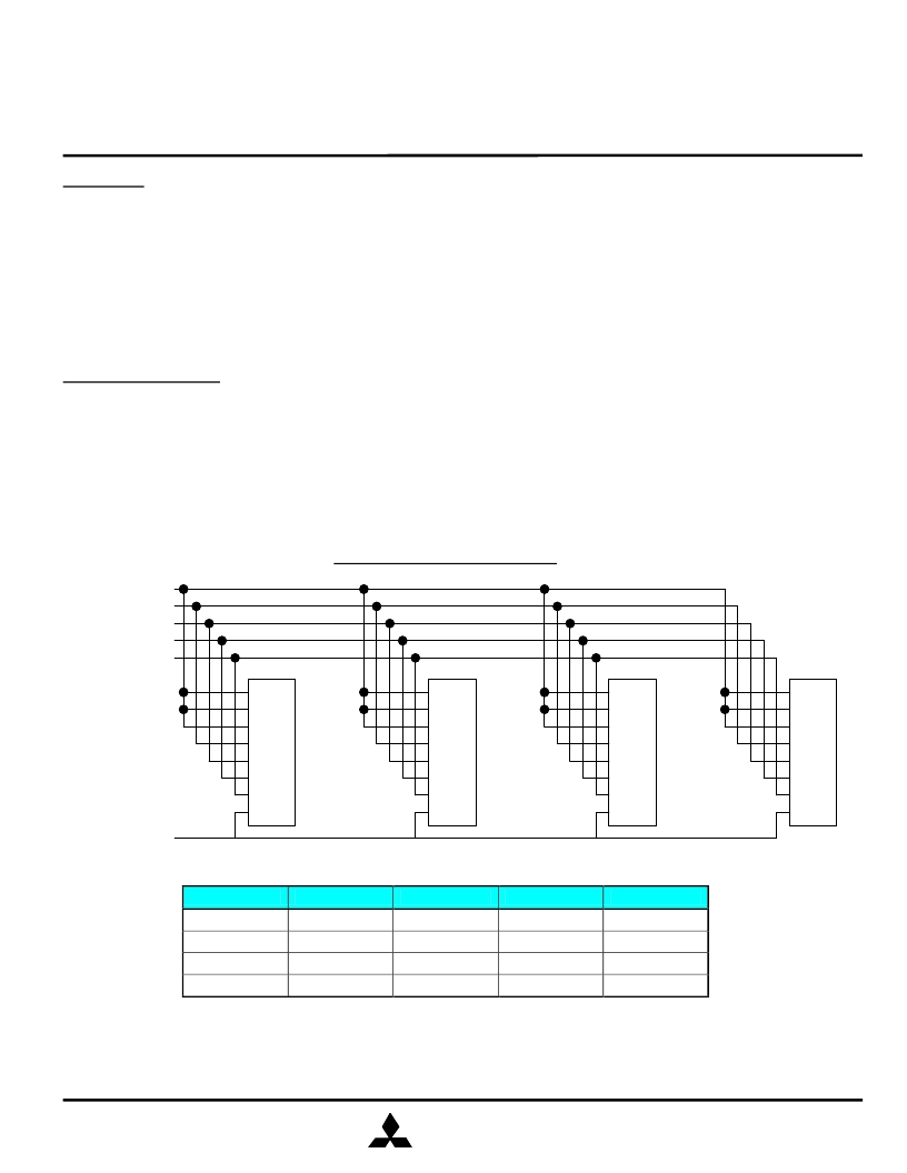
Programmability of E2 and E3 allows for banks of depth expansion to be accomplished with no additional logic. By programming the
enable inputs of four SRAMs in binary sequence (00,01,10,11) and driving the enable inputs with two address inputs, four SRAMs can
be made to look like one larger SRAM to the system.
Bank Enable Truth Table
EP2
EP3
E2
E3
Bank0
Bank1
Bank2
Bank3
LOW
LOW
HIGH
HIGH
LOW
HIGH
LOW
HIGH
Active Low
Active Low
Active High
Active High
Active Low
Active High
Active Low
Active High
A
E3#
E2#
E1#
CK
W#
DQ
CQ
Bank0
A
0
~A
19
7E1#
CK
W#
DQa~DQh
A
0
~A
17
A
18
A
19
A
E3
E2#
E1#
CK
W#
DQ
CQ
Bank1
A
0
~A
17
A
18
A
19
A
E3#
E2
E1#
CK
W#
DQ
CQ
Bank2
A
0
~A
17
A
18
A
19
A
E3
E2
E1#
CK
W#
DQ
CQ
Bank3
A
0
~A
17
A
18
A
19
CQ
Example Four Bank Depth Schematic
相关PDF资料 |
PDF描述 |
|---|---|
| M5M5Y5672TG-22 | 18874368-BIT(262144-WORD BY 72-BIT) NETWORK SRAM |
| M5M5Y5672TG-25 | 18874368-BIT(262144-WORD BY 72-BIT) NETWORK SRAM |
| M5M5Y816WG-70HI | 8388608-BIT (524288-WORD BY 16-BIT) CMOS STATIC RAM |
| M5M5Y816WG-85HI | 8388608-BIT (524288-WORD BY 16-BIT) CMOS STATIC RAM |
| M5M82C59AFP | The M5M82C59AFP,-2 is programmable LSI Interupt control |
相关代理商/技术参数 |
参数描述 |
|---|---|
| M5M80011A | 制造商:Mitsubishi Electric 功能描述: |
| M5M82C54P | 制造商:MITSUBISHI 制造商全称:Mitsubishi Electric Semiconductor 功能描述:CMOS PROGRAMMABLE INTERVAL TIMER |
| M5M82C54P-6 | 制造商:MITSUBISHI 制造商全称:Mitsubishi Electric Semiconductor 功能描述:CMOS PROGRAMMABLE INTERVAL TIMER |
| M5M82C55AFP2 | 制造商:Panasonic Industrial Company 功能描述:IC |
| M5M82C59AFP | 制造商:MITSUBISHI 制造商全称:Mitsubishi Electric Semiconductor 功能描述:The M5M82C59AFP,-2 is programmable LSI Interupt control |
发布紧急采购,3分钟左右您将得到回复。