- 您现在的位置:买卖IC网 > PDF目录1849 > MAX8792ETD+T (Maxim Integrated Products)IC PWM CTRLR STEP-DWN 14TDFN PDF资料下载
参数资料
| 型号: | MAX8792ETD+T |
| 厂商: | Maxim Integrated Products |
| 文件页数: | 19/28页 |
| 文件大小: | 0K |
| 描述: | IC PWM CTRLR STEP-DWN 14TDFN |
| 产品培训模块: | Lead (SnPb) Finish for COTS Obsolescence Mitigation Program |
| 标准包装: | 1 |
| 应用: | PWM 控制器 |
| 输入电压: | 2 V ~ 26 V |
| 电源电压: | 4.5 V ~ 5.5 V |
| 电流 - 电源: | 700µA |
| 工作温度: | -40°C ~ 85°C |
| 安装类型: | 表面贴装 |
| 封装/外壳: | 14-WFDFN 裸露焊盘 |
| 供应商设备封装: | 14-TDFN-EP(3x3) |
| 包装: | 标准包装 |
| 其它名称: | MAX8792ETD+TDKR |
第1页第2页第3页第4页第5页第6页第7页第8页第9页第10页第11页第12页第13页第14页第15页第16页第17页第18页当前第19页第20页第21页第22页第23页第24页第25页第26页第27页第28页
�� �
�
�Single� Quick-PWM� Step-Down�
�Controller� with� Dynamic� REFIN�
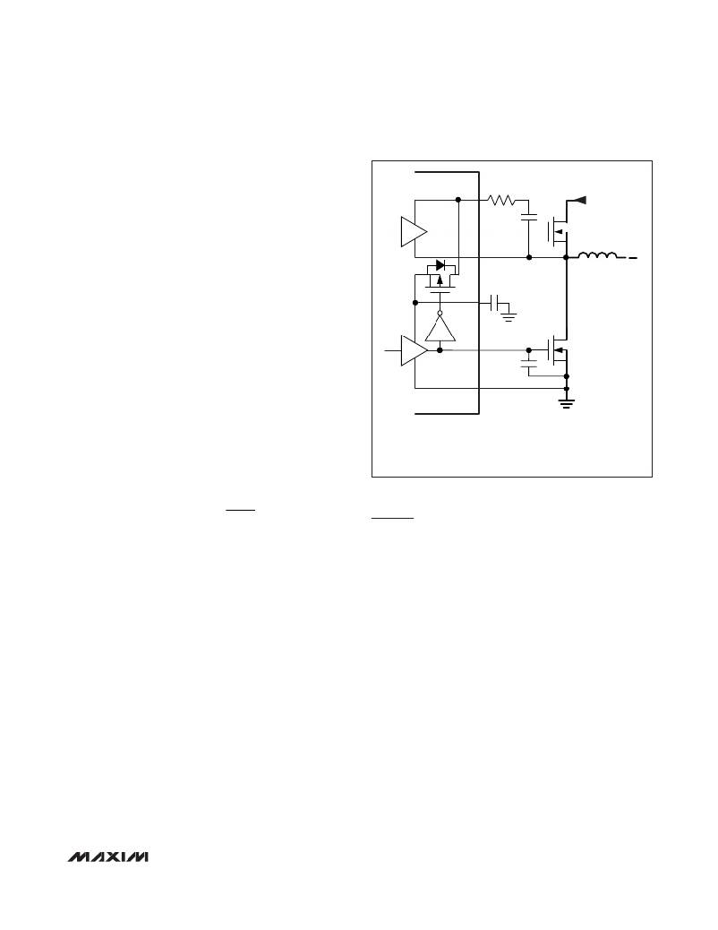
�Adaptive� dead-time� circuits� monitor� the� DL� and� DH� dri-�
�vers� and� prevent� either� FET� from� turning� on� until� the�
�other� is� fully� off.� The� adaptive� driver� dead� time� allows�
�operation� without� shoot-through� with� a� wide� range� of�
�MOSFETs,� minimizing� delays� and� maintaining� efficiency.�
�There� must� be� a� low-resistance,� low-inductance� path�
�from� the� DL� and� DH� drivers� to� the� MOSFET� gates� for�
�the� adaptive� dead-time� circuits� to� work� properly;� other-�
�BST�
�DH�
�LX�
�(R� BST� )*�
�C� BST�
�N� H�
�INPUT� (V� IN� )�
�L�
�wise,� the� sense� circuitry� in� the� MAX8792� interprets� the�
�MOSFET� gates� as� “off”� while� charge� actually� remains.�
�Use� very� short,� wide� traces� (50� mils� to� 100� mils� wide� if�
�the� MOSFET� is� 1in� from� the� driver).�
�The� internal� pulldown� transistor� that� drives� DL� low� is�
�robust,� with� a� 0.9� Ω� (typ)� on-resistance.� This� helps� pre-�
�vent� DL� from� being� pulled� up� due� to� capacitive� coupling�
�V� DD�
�DL�
�C� BYP�
�N� L�
�V� GS� (� TH� )� >� V� IN� ?� RSS� ?�
�from the drain to the gate of the low-side MOSFETs�
�when� the� inductor� node� (LX)� quickly� switches� from�
�ground� to� V� IN� .� Applications� with� high-input� voltages� and�
�long� inductive� driver� traces� may� require� rising� LX� edges�
�do� not� pull� up� the� low-side� MOSFETs’� gate,� causing�
�shoot-through� currents.� The� capacitive� coupling�
�between� LX� and� DL� created� by� the� MOSFET’s� gate-to-�
�drain� capacitance� (C� RSS� ),� gate-to-source� capacitance�
�(C� ISS� -� C� RSS� ),� and� additional� board� parasitics� should�
�not� exceed� the� following� minimum� threshold:�
�?� C� ?�
�?� C� ISS� ?�
�Typically,� adding� a� 4700pF� between� DL� and� power�
�ground� (C� NL� in� Figure� 6),� close� to� the� low-side�
�MOSFETs,� greatly� reduces� coupling.� Do� not� exceed�
�22nF� of� total� gate� capacitance� to� prevent� excessive�
�turn-off� delays.�
�(C� NL� )*�
�PGND�
�(R� BST� )*� OPTIONAL—THE� RESISTOR� LOWERS� EMI� BY� DECREASING�
�THE� SWITCHING� NODE� RISE� TIME.�
�(C� NL� )*� OPTIONAL—THE� CAPACITOR� REDUCES� LX� TO� DL� CAPACITIVE�
�COUPLING� THAT� CAN� CAUSE� SHOOT-THROUGH� CURRENTS.�
�Figure� 6.� Gate� Drive� Circuit�
�Quick-PWM� Design� Procedure�
�Firmly� establish� the� input� voltage� range� and� maximum�
�load� current� before� choosing� a� switching� frequency� and�
�inductor� operating� point� (ripple-current� ratio).� The� prima-�
�ry� design� trade-off� lies� in� choosing� a� good� switching� fre-�
�quency� and� inductor� operating� point,� and� the� following�
�four� factors� dictate� the� rest� of� the� design:�
�Alternatively,� shoot-through� currents� can� be� caused� by�
�a� combination� of� fast� high-side� MOSFETs� and� slow� low-�
�side� MOSFETs.� If� the� turn-off� delay� time� of� the� low-side�
�MOSFET� is� too� long,� the� high-side� MOSFETs� can� turn�
�on� before� the� low-side� MOSFETs� have� actually� turned�
�off.� Adding� a� resistor� less� than� 5� Ω� in� series� with� BST�
�slows� down� the� high-side� MOSFET� turn-on� time,� elimi-�
�nating� the� shoot-through� currents� without� degrading�
�the� turn-off� time� (R� BST� in� Figure� 6).� Slowing� down� the�
�high-side� MOSFET� also� reduces� the� LX� node� rise� time,�
�thereby� reducing� EMI� and� high-frequency� coupling�
�responsible� for� switching� noise.�
�?�
�?�
�Input� voltage� range:� The� maximum� value�
�(V� IN(MAX)� )� must� accommodate� the� worst-case� input�
�supply� voltage� allowed� by� the� notebook� ’s� AC�
�adapter� voltage.� The� minimum� value� (V� IN(MIN)� )�
�must� account� for� the� lowest� input� voltage� after�
�drops� due� to� connectors,� fuses,� and� battery� selec-�
�tor� switches.� If� there� is� a� choice� at� all,� lower� input�
�voltages� result� in� better� efficiency.�
�Maximum� load� current:� There� are� two� values� to�
�consider.� The� peak� load� current� (I� LOAD(MAX)� )�
�determines� the� instantaneous� component� stresses�
�and� filtering� requirements,� and� thus� drives� output�
�______________________________________________________________________________________�
�19�
�相关PDF资料 |
PDF描述 |
|---|---|
| MAX8794ETB+T | IC DDR LINEAR REG 10-TDFN |
| MAX8795AETJ+C7P | IC TFT-LCD DC/DC CONV 32-TQFN |
| MAX8798ETX+T | IC INTERNAL-SW BOOST REG 36-TQFN |
| MAX8804VETA+T | IC USB/AC ADP CHARGER 8TDFN-EP |
| MAX8804YETA+T | IC USB/AC ADP CHARGER 8-TDFN |
相关代理商/技术参数 |
参数描述 |
|---|---|
| MAX8792EVKIT+ | 功能描述:电源管理IC开发工具 MAX8792 Eval Kit RoHS:否 制造商:Maxim Integrated 产品:Evaluation Kits 类型:Battery Management 工具用于评估:MAX17710GB 输入电压: 输出电压:1.8 V |
| MAX8794ETB/V+T | 功能描述:低压差稳压器 - LDO Low-Voltage DDR Linear Regulator RoHS:否 制造商:Texas Instruments 最大输入电压:36 V 输出电压:1.4 V to 20.5 V 回动电压(最大值):307 mV 输出电流:1 A 负载调节:0.3 % 输出端数量: 输出类型:Fixed 最大工作温度:+ 125 C 安装风格:SMD/SMT 封装 / 箱体:VQFN-20 |
| MAX8794ETB+ | 制造商:Maxim Integrated Products 功能描述: 制造商:Maxim Integrated Products 功能描述:LOW-VOLTAGE DDR LINEAR REGULATOR - Rail/Tube |
| MAX8794ETB+T | 功能描述:低压差稳压器 - LDO Low-Voltage DDR Linear Regulator RoHS:否 制造商:Texas Instruments 最大输入电压:36 V 输出电压:1.4 V to 20.5 V 回动电压(最大值):307 mV 输出电流:1 A 负载调节:0.3 % 输出端数量: 输出类型:Fixed 最大工作温度:+ 125 C 安装风格:SMD/SMT 封装 / 箱体:VQFN-20 |
| MAX8795AETJ+ | 功能描述:直流/直流开关转换器 TFT-LCD DC/DC Converter RoHS:否 制造商:STMicroelectronics 最大输入电压:4.5 V 开关频率:1.5 MHz 输出电压:4.6 V 输出电流:250 mA 输出端数量:2 最大工作温度:+ 85 C 安装风格:SMD/SMT |
发布紧急采购,3分钟左右您将得到回复。