- 您现在的位置:买卖IC网 > PDF目录69025 > MC68CK338CPV14B1 (FREESCALE SEMICONDUCTOR INC) 32-BIT, 14.4 MHz, MICROCONTROLLER, PQFP144 PDF资料下载
参数资料
| 型号: | MC68CK338CPV14B1 |
| 厂商: | FREESCALE SEMICONDUCTOR INC |
| 元件分类: | 微控制器/微处理器 |
| 英文描述: | 32-BIT, 14.4 MHz, MICROCONTROLLER, PQFP144 |
| 封装: | PLASTIC, TQFP-144 |
| 文件页数: | 122/133页 |
| 文件大小: | 944K |
| 代理商: | MC68CK338CPV14B1 |
第1页第2页第3页第4页第5页第6页第7页第8页第9页第10页第11页第12页第13页第14页第15页第16页第17页第18页第19页第20页第21页第22页第23页第24页第25页第26页第27页第28页第29页第30页第31页第32页第33页第34页第35页第36页第37页第38页第39页第40页第41页第42页第43页第44页第45页第46页第47页第48页第49页第50页第51页第52页第53页第54页第55页第56页第57页第58页第59页第60页第61页第62页第63页第64页第65页第66页第67页第68页第69页第70页第71页第72页第73页第74页第75页第76页第77页第78页第79页第80页第81页第82页第83页第84页第85页第86页第87页第88页第89页第90页第91页第92页第93页第94页第95页第96页第97页第98页第99页第100页第101页第102页第103页第104页第105页第106页第107页第108页第109页第110页第111页第112页第113页第114页第115页第116页第117页第118页第119页第120页第121页当前第122页第123页第124页第125页第126页第127页第128页第129页第130页第131页第132页第133页
MC68CK338
MOTOROLA
MC68CK338TS/D
89
IL[2:0] — Interrupt Level
Setting IL[2:0] to a non-zero value causes the FCSM to request an interrupt of the selected level when
the COF bit sets. If IL[2:0] = %000, no interrupt will be requested when COF sets. These bits can be
read or written at any time and are cleared by reset.
IARB3 — Interrupt Arbitration Bit 3
This bit works in conjunction with IARB[2:0] in the BIUMCR. Each module that generates interrupt re-
quests on the IMB must have a unique value in the arbitration field. This interrupt arbitration identifica-
tion number is used to arbitrate for the IMB when modules generate simultaneous interrupts of the same
priority. The IARB3 bit is cleared by reset. Refer to 6.4.1 BIUSM Registers for more information on
IARB[2:0].
DRV[A:B] — Drive Time Base Bus
This bit field contains read/write bits that control the connection of the FCSM to the time base buses A
and B. These bits are cleared by reset. Refer to Table 52.
WARNING
Two time base buses should not be driven at the same time.
IN — Input Pin Status Bit
This read-only status bit reflects the logic state of the FCSM input pin. Writing to this bit has no effect,
nor does reset.
NOTE
The clock input of FCSM3 is internally connected to I/O pin CTD27 of DASM27 and
will read the state of that pin.
CLK[2:0] — Counter Clock Select
These read/write control bits select one of six internal clock signals (PCLK[1:6]) or one of two external
conditions on the external clock input pin. Maximum frequency of the external clock signals is fsys/4.
Refer to Table 54.
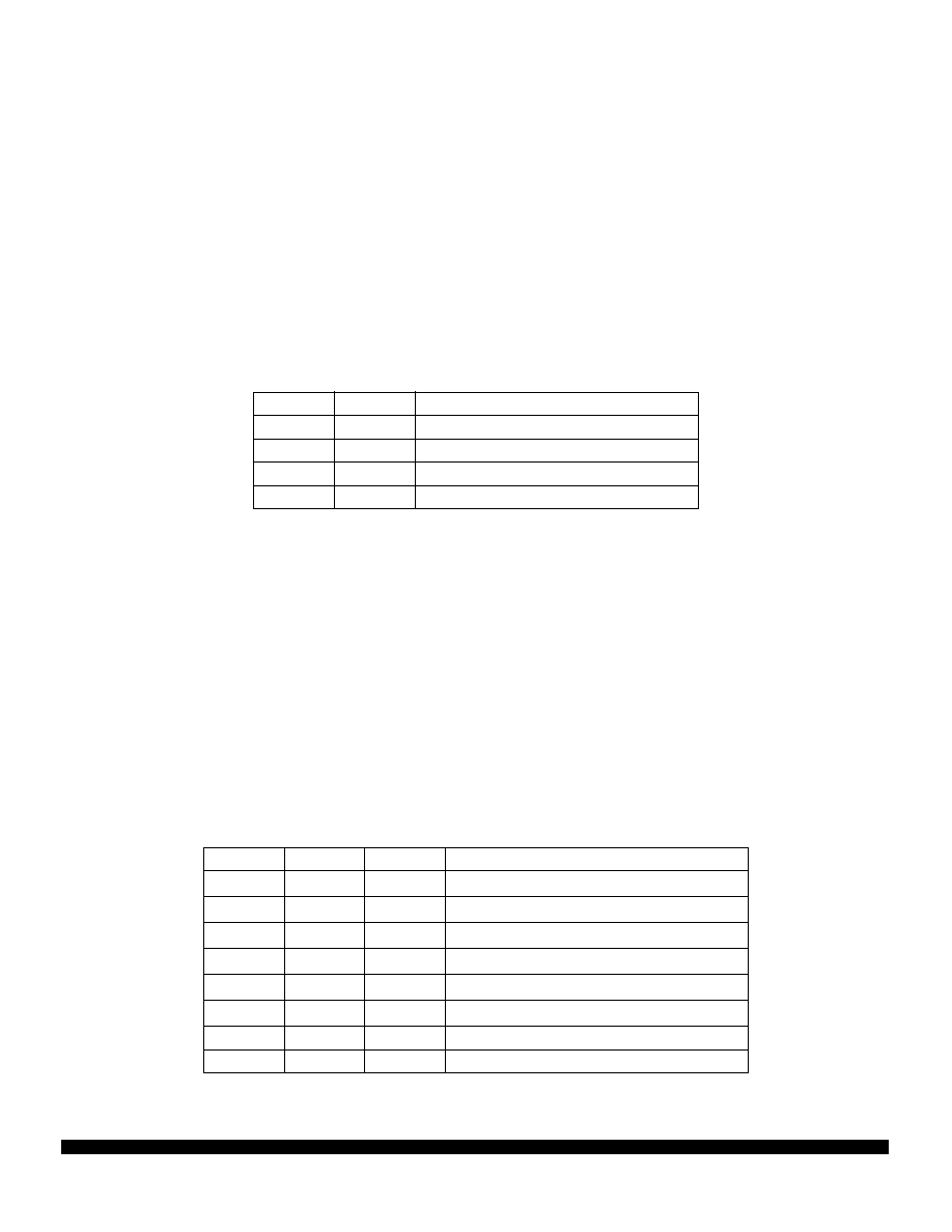
Table 50 Drive Time Base Bus Field
DRVA
DRVB
Bus Selected
0
No time base bus driven
0
1
Time base bus B is driven
1
0
Time base bus A is driven
1
Both time base buses A and B are driven
Table 51 Counter Clock Select Field
CLK2
CLK1
CLK0
Free-Running Counter Clock Source
000
PCLK1 (fsys ÷ 2 or fsys ÷ 3)
001
PCLK2 (fsys ÷ 4 or fsys ÷ 6)
010
PCLK3 (fsys ÷ 8 or fsys ÷ 12)
011
PCLK4 (fsys ÷ 16 or fsys ÷ 24)
100
PCLK5 (fsys ÷ 32 or fsys ÷ 48)
101
PCLK6 (fsys ÷ 64 or fsys ÷ 768)
1
0
External clock input, falling edge
1
External clock input, rising edge
F
re
e
sc
a
le
S
e
m
ic
o
n
d
u
c
to
r,
I
Freescale Semiconductor, Inc.
For More Information On This Product,
Go to: www.freescale.com
n
c
..
.
相关PDF资料 |
PDF描述 |
|---|---|
| MC68CK338CPV14 | 32-BIT, 14.4 MHz, MICROCONTROLLER, PQFP144 |
| MC68EN360CRC25 | 32-BIT, 25 MHz, RISC MICROCONTROLLER, CPGA241 |
| MC68F333FE | 32-BIT, FLASH, 16.78 MHz, MICROCONTROLLER, CQFP160 |
| MC68F333FC | 32-BIT, FLASH, 16.78 MHz, MICROCONTROLLER, PQFP160 |
| MC68HC000L12F | 16-BIT, 16.67 MHz, MICROPROCESSOR, CDIP64 |
相关代理商/技术参数 |
参数描述 |
|---|---|
| MC68CM16Z1 | 制造商:FREESCALE 制造商全称:Freescale Semiconductor, Inc 功能描述:M68HC16Z Series |
| MC68CM16Z1CFC16 | 制造商:FREESCALE 制造商全称:Freescale Semiconductor, Inc 功能描述:M68HC16Z Series |
| MC68CM16Z1CPV16 | 制造商:FREESCALE 制造商全称:Freescale Semiconductor, Inc 功能描述:M68HC16Z Series |
| MC68E360VR25VLR2 | 功能描述:微处理器 - MPU QUICC ETHRN RoHS:否 制造商:Atmel 处理器系列:SAMA5D31 核心:ARM Cortex A5 数据总线宽度:32 bit 最大时钟频率:536 MHz 程序存储器大小:32 KB 数据 RAM 大小:128 KB 接口类型:CAN, Ethernet, LIN, SPI,TWI, UART, USB 工作电源电压:1.8 V to 3.3 V 最大工作温度:+ 85 C 安装风格:SMD/SMT 封装 / 箱体:FBGA-324 |
| MC68E360ZP25VLR2 | 功能描述:IC MPU QUICC 32BIT 357-PBGA RoHS:否 类别:集成电路 (IC) >> 嵌入式 - 微处理器 系列:M683xx 标准包装:1 系列:MPC85xx 处理器类型:32-位 MPC85xx PowerQUICC III 特点:- 速度:1.2GHz 电压:1.1V 安装类型:表面贴装 封装/外壳:783-BBGA,FCBGA 供应商设备封装:783-FCPBGA(29x29) 包装:托盘 |
发布紧急采购,3分钟左右您将得到回复。