- 您现在的位置:买卖IC网 > PDF目录67968 > MC7455ARX867LG (MOTOROLA INC) 32-BIT, 867 MHz, RISC PROCESSOR, CBGA483 PDF资料下载
参数资料
| 型号: | MC7455ARX867LG |
| 厂商: | MOTOROLA INC |
| 元件分类: | 微控制器/微处理器 |
| 英文描述: | 32-BIT, 867 MHz, RISC PROCESSOR, CBGA483 |
| 封装: | 29 X 29 MM, 1.27 MM PITCH, CERAMIC, BGA-483 |
| 文件页数: | 14/76页 |
| 文件大小: | 1520K |
| 代理商: | MC7455ARX867LG |
第1页第2页第3页第4页第5页第6页第7页第8页第9页第10页第11页第12页第13页当前第14页第15页第16页第17页第18页第19页第20页第21页第22页第23页第24页第25页第26页第27页第28页第29页第30页第31页第32页第33页第34页第35页第36页第37页第38页第39页第40页第41页第42页第43页第44页第45页第46页第47页第48页第49页第50页第51页第52页第53页第54页第55页第56页第57页第58页第59页第60页第61页第62页第63页第64页第65页第66页第67页第68页第69页第70页第71页第72页第73页第74页第75页第76页
MOTOROLA
MPC7455 RISC Microprocessor Hardware Specifications
21
Electrical and Thermal Characteristics
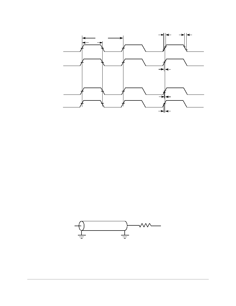
The L3_CLK timing diagram is shown in Figure 7.
Figure 7. L3_CLK_OUT Output Timing Diagram
1.5.2.4
L3 Bus AC Specifications
The MPC7455 L3 interface supports three different types of SRAM: source-synchronous, double data rate
(DDR) MSUG2 SRAM, late write SRAMs, and pipeline burst (PB2) SRAMs. Each requires a different
protocol on the L3 interface and a different routing of the L3 clock signals. The type of SRAM is
programmed in L3CR[22:23] and the MPC7455 then follows the appropriate protocol for that type. The
designer must connect and route the L3 signals appropriately for each type of SRAM. Following are some
observations about the chip-to-SRAM interface.
The routing for the point-to-point signals (L3_CLK[0:1], L3DATA[0:63], L3DP[0:7], and
L3_ECHO_CLK[0:3]) to a particular SRAM should be delay matched. If necessary, the length of
traces can be altered in order to intentionally skew the timing and provide additional setup or hold
time margin.
For a 1-Mbyte L3, use address bits 16:0 (bit 0 is LSB).
No pull-up resistors are required for the L3 interface.
For high speed operations, L3 interface address and control signals should be a ‘T’ with minimal
stubs to the two loads; data and clock signals should be point-to-point to their single load. Figure 8
shows the AC test load for the L3 interface.
Figure 8. AC Test Load for the L3 Interface
In general, if routing is short, delay-matched, and designed for incident wave reception and minimal
reflection, there is a high probability that the AC timing of the MPC7455 L3 interface will meet the
maximum frequency operation of appropriately chosen SRAMs. This is despite the pessimistic,
guard-banded AC specifications (see Table 12, Table 13, and Table 14), the limitations of functional testers
L3_CLK0
VM
tL3CR
tL3CF
VM
L3_CLK1
VM
tL3_CLK
tCHCL
VM
tL3CSKW1
L3_ECHO_CLK1
L3_ECHO_CLK3
VM
tL3CSKW2
VM
tL3CSKW2
For PB2 or Late Write:
Output
Z0 = 50
GVDD/2
RL = 50
相关PDF资料 |
PDF描述 |
|---|---|
| MC7445ARX733LG | 32-BIT, 733 MHz, RISC PROCESSOR, CBGA360 |
| MC7445ARX1000LG | 32-BIT, 1000 MHz, RISC PROCESSOR, CBGA360 |
| MC7445ARX933LG | 32-BIT, 933 MHz, RISC PROCESSOR, CBGA360 |
| MC7455ARX1000LG | 32-BIT, 1000 MHz, RISC PROCESSOR, CBGA483 |
| MC7455ARX933LG | 32-BIT, 933 MHz, RISC PROCESSOR, CBGA483 |
相关代理商/技术参数 |
参数描述 |
|---|---|
| MC7455ARX933LF | 制造商:FREESCALE 制造商全称:Freescale Semiconductor, Inc 功能描述:RISC Microprocessor Hardware Specifications |
| MC7455ARX933LG | 制造商:FREESCALE 制造商全称:Freescale Semiconductor, Inc 功能描述:RISC Microprocessor Hardware Specifications |
| MC7457RX1000LC | 功能描述:微处理器 - MPU APOLO7 RV1.2 1.3V 105C RoHS:否 制造商:Atmel 处理器系列:SAMA5D31 核心:ARM Cortex A5 数据总线宽度:32 bit 最大时钟频率:536 MHz 程序存储器大小:32 KB 数据 RAM 大小:128 KB 接口类型:CAN, Ethernet, LIN, SPI,TWI, UART, USB 工作电源电压:1.8 V to 3.3 V 最大工作温度:+ 85 C 安装风格:SMD/SMT 封装 / 箱体:FBGA-324 |
| MC7457RX1000NB | 制造商:Motorola Inc 功能描述: |
| MC7457RX1000NC | 功能描述:微处理器 - MPU APOLO7 RV1.2 1.1V 105C RoHS:否 制造商:Atmel 处理器系列:SAMA5D31 核心:ARM Cortex A5 数据总线宽度:32 bit 最大时钟频率:536 MHz 程序存储器大小:32 KB 数据 RAM 大小:128 KB 接口类型:CAN, Ethernet, LIN, SPI,TWI, UART, USB 工作电源电压:1.8 V to 3.3 V 最大工作温度:+ 85 C 安装风格:SMD/SMT 封装 / 箱体:FBGA-324 |
发布紧急采购,3分钟左右您将得到回复。