- 您现在的位置:买卖IC网 > PDF目录67968 > MC7455ARX867LG (MOTOROLA INC) 32-BIT, 867 MHz, RISC PROCESSOR, CBGA483 PDF资料下载
参数资料
| 型号: | MC7455ARX867LG |
| 厂商: | MOTOROLA INC |
| 元件分类: | 微控制器/微处理器 |
| 英文描述: | 32-BIT, 867 MHz, RISC PROCESSOR, CBGA483 |
| 封装: | 29 X 29 MM, 1.27 MM PITCH, CERAMIC, BGA-483 |
| 文件页数: | 15/76页 |
| 文件大小: | 1520K |
| 代理商: | MC7455ARX867LG |
第1页第2页第3页第4页第5页第6页第7页第8页第9页第10页第11页第12页第13页第14页当前第15页第16页第17页第18页第19页第20页第21页第22页第23页第24页第25页第26页第27页第28页第29页第30页第31页第32页第33页第34页第35页第36页第37页第38页第39页第40页第41页第42页第43页第44页第45页第46页第47页第48页第49页第50页第51页第52页第53页第54页第55页第56页第57页第58页第59页第60页第61页第62页第63页第64页第65页第66页第67页第68页第69页第70页第71页第72页第73页第74页第75页第76页
22
MPC7455 RISC Microprocessor Hardware Specifications
MOTOROLA
Electrical and Thermal Characteristics
described in Section 1.5.2.3, “L3 Clock AC Specifications,” and the uncertainty of clocks and signals which
inevitably make worst-case critical path timing analysis pessimistic.
More specifically, certain signals within groups should be delay-matched with others in the same group
while intergroup routing is less critical. Only the address and control signals are common to both SRAMs
and additional timing margin is available for these signals. The double-clocked data signals are grouped
with individual clocks as shown in Figure 9 or Figure 11, depending on the type of SRAM. For example,
for the MSUG2 DDR SRAM (see Figure 9); L3DATA[0:31], L3DP[0:3], and L3_CLK[0] form a closely
coupled group of outputs from the MPC7455; while L3DATA[0:15], L3DP[0:1], and L3_ECHO_CLK[0]
form a closely coupled group of inputs.
The MPC7450 RISC Microprocessor Family User’s Manual refers to logical settings called ‘sample points’
used in the synchronization of reads from the receive FIFO. The computation of the correct value for this
setting is system-dependent and is described in the MPC7450 RISC Microprocessor Family User’s Manual.
Three specifications are used in this calculation and are given in Table 11. It is essential that all three
specifications are included in the calculations to determine the sample points, as incorrect settings can result
in errors and unpredictable behavior. For more information, see the MPC7450 RISC Microprocessor Family
User’s Manual.
1.5.2.4.1
L3 Bus AC Specifications for DDR MSUG2 SRAMs
When using DDR MSUG2 SRAMs at the L3 interface, the parts should be connected as shown in Figure 9.
Outputs from the MPC7455 are actually launched on the edges of an internal clock phase-aligned to
SYSCLK (adjusted for core and L3 frequency divisors). L3_CLK0 and L3_CLK1 are this internal clock
output with 90° phase delay, so outputs are shown synchronous to L3_CLK0 and L3_CLK1. Output valid
times are typically negative when referenced to L3_CLKn because the data is launched one-quarter period
before L3_CLKn to provide adequate setup time at the SRAM after the delay-matched address, control,
data, and L3_CLKn signals have propagated across the printed-wiring board.
Inputs to the MPC7455 are source-synchronous with the CQ clock generated by the DDR MSUG2 SRAMs.
These CQ clocks are received on the L3_ECHO_CLKn inputs of the MPC7455. An internal circuit delays
the incoming L3_ECHO_CLKn signal such that it is positioned within the valid data window at the internal
receiving latches. This delayed clock is used to capture the data into these latches which comprise the
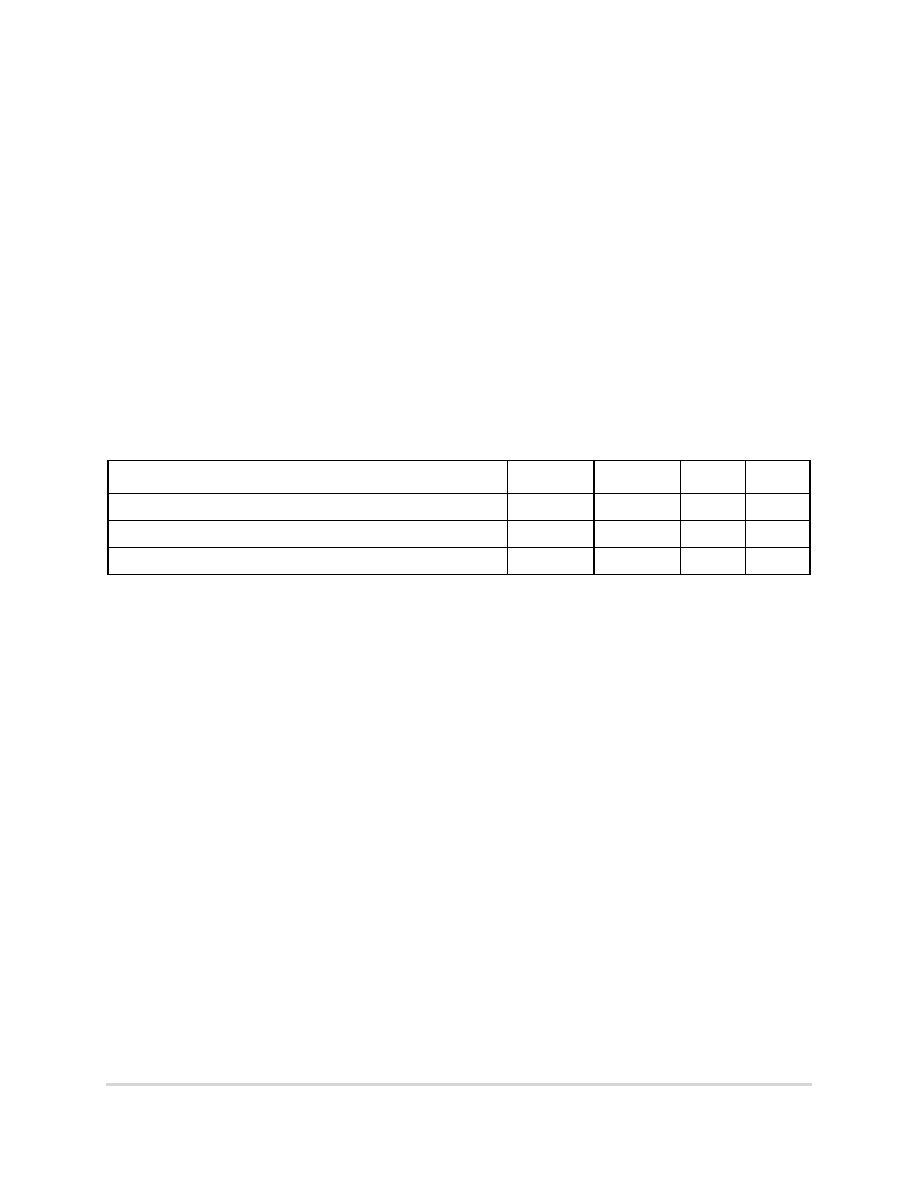
Table 11. Sample Points Calculation Parameters
Parameter
Symbol
Max
Unit
Notes
Delay from processor clock to internal_L3_CLK
tAC
3/4
tL3_CLK
1
Delay from internal_L3_CLK to L3_CLKn output pins
tCO
3ns
2
Delay from L3_ECHO_CLKn to receive latch
tECI
3ns
3
Notes:
1. This specification describes a logical offset between the internal clock edge used to launch the L3 address and
control signals (this clock edge is phase-aligned with the processor clock edge) and the internal clock edge used
to launch the L3_CLKn signals. With proper board routing, this offset ensures that the L3_CLKn edge will arrive at
the SRAM within a valid address window and provide adequate setup and hold time. This offset is reflected in the
L3 bus interface AC timing specifications, but must also be separately accounted for in the calculation of sample
points and, thus, is specified here.
2. This specification is the delay from a rising or falling edge on the internal_L3_CLK signal to the corresponding
rising or falling edge at the L3CLKn pins.
3. This specification is the delay from a rising or falling edge of L3_ECHO_CLKn to data valid and ready to be
sampled from the FIFO.
相关PDF资料 |
PDF描述 |
|---|---|
| MC7445ARX733LG | 32-BIT, 733 MHz, RISC PROCESSOR, CBGA360 |
| MC7445ARX1000LG | 32-BIT, 1000 MHz, RISC PROCESSOR, CBGA360 |
| MC7445ARX933LG | 32-BIT, 933 MHz, RISC PROCESSOR, CBGA360 |
| MC7455ARX1000LG | 32-BIT, 1000 MHz, RISC PROCESSOR, CBGA483 |
| MC7455ARX933LG | 32-BIT, 933 MHz, RISC PROCESSOR, CBGA483 |
相关代理商/技术参数 |
参数描述 |
|---|---|
| MC7455ARX933LF | 制造商:FREESCALE 制造商全称:Freescale Semiconductor, Inc 功能描述:RISC Microprocessor Hardware Specifications |
| MC7455ARX933LG | 制造商:FREESCALE 制造商全称:Freescale Semiconductor, Inc 功能描述:RISC Microprocessor Hardware Specifications |
| MC7457RX1000LC | 功能描述:微处理器 - MPU APOLO7 RV1.2 1.3V 105C RoHS:否 制造商:Atmel 处理器系列:SAMA5D31 核心:ARM Cortex A5 数据总线宽度:32 bit 最大时钟频率:536 MHz 程序存储器大小:32 KB 数据 RAM 大小:128 KB 接口类型:CAN, Ethernet, LIN, SPI,TWI, UART, USB 工作电源电压:1.8 V to 3.3 V 最大工作温度:+ 85 C 安装风格:SMD/SMT 封装 / 箱体:FBGA-324 |
| MC7457RX1000NB | 制造商:Motorola Inc 功能描述: |
| MC7457RX1000NC | 功能描述:微处理器 - MPU APOLO7 RV1.2 1.1V 105C RoHS:否 制造商:Atmel 处理器系列:SAMA5D31 核心:ARM Cortex A5 数据总线宽度:32 bit 最大时钟频率:536 MHz 程序存储器大小:32 KB 数据 RAM 大小:128 KB 接口类型:CAN, Ethernet, LIN, SPI,TWI, UART, USB 工作电源电压:1.8 V to 3.3 V 最大工作温度:+ 85 C 安装风格:SMD/SMT 封装 / 箱体:FBGA-324 |
发布紧急采购,3分钟左右您将得到回复。