- 您现在的位置:买卖IC网 > PDF目录26811 > MC88915TFN160R2 (MOTOROLA INC) 88915 SERIES, PLL BASED CLOCK DRIVER, 7 TRUE OUTPUT(S), 1 INVERTED OUTPUT(S), PQCC28 PDF资料下载
参数资料
| 型号: | MC88915TFN160R2 |
| 厂商: | MOTOROLA INC |
| 元件分类: | 时钟及定时 |
| 英文描述: | 88915 SERIES, PLL BASED CLOCK DRIVER, 7 TRUE OUTPUT(S), 1 INVERTED OUTPUT(S), PQCC28 |
| 封装: | PLASTIC, LCC-28 |
| 文件页数: | 10/19页 |
| 文件大小: | 181K |
| 代理商: | MC88915TFN160R2 |
MC88915T
MOTOROLA ADVANCED CLOCK DRIVERS DEVICE DATA
29
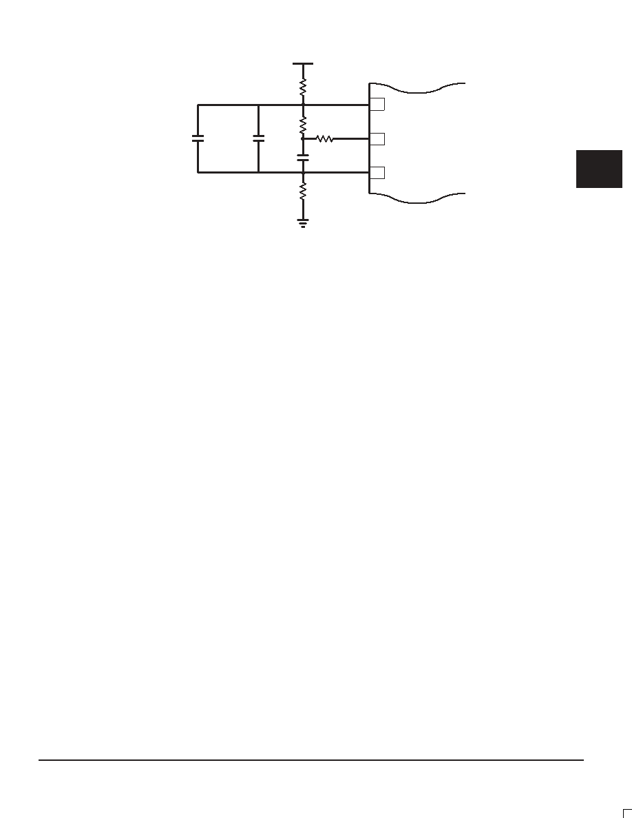
Figure 6. Recommended Loop Filter and Analog Isolation Scheme for the MC88915T
47
BOARD VCC
0.1F (LOOP
FILTER CAP)
330
1M
0.1F HIGH
FREQ
BYPASS
10F LOW
FREQ BYPASS
47
BOARD GND
8
9
10
ANALOG VCC
RC1
ANALOG GND
ANALOG LOOP FILTER/VCO
SECTION OF THE MC88915T
28-PIN PLCC PACKAGE (NOT
DRAWN TO SCALE)
A SEPARATE ANALOG POWER SUPPLY IS NOT NECESSARY AND
SHOULDNOT BE USED. FOLLOWING THESE PRESCRIBED GUIDELINES
IS ALL THAT IS NECESSARY TO USE THE MC88915T IN A NORMAL
DIGITAL ENVIRONMENT.
Notes Concerning Loop Filter and Board Layout Issues
1. Figure 6 shows a loop filter and analog isolation scheme
which will be effective in most applications. The following
guidelines should be followed to ensure stable and
jitter–free operation:
1a.All loop filter and analog isolation components should be
tied as close to the package as possible. Stray current
passing through the parasitics of long traces can cause
undesirable voltage transients at the RC1 pin.
1b.The 47
resistors, the 10F low frequency bypass
capacitor, and the 0.1
F high frequency bypass capacitor
form a wide bandwidth filter that will minimize the 88915T’s
sensitivity to voltage transients from the system digital VCC
supply and ground planes. This filter will typically ensure
that a 100mV step deviation on the digital VCC supply will
cause no more than a 100pS phase deviation on the
88915T outputs. A 250mV step deviation on VCC using the
recommended filter values should cause no more than a
250pS phase deviation; if a 25
F bypass capacitor is used
(instead of 10
F) a 250mV VCC step should cause no more
than a 100pS phase deviation.
If good bypass techniques are used on a board design near
components which may cause digital VCC and ground
noise, the above described VCC step deviations should not
occur at the 88915T’s digital VCC supply. The purpose of
the bypass filtering scheme shown in Figure 6 is to give the
88915T additional protection from the power supply and
ground plane transients that can occur in a high frequency,
high speed digital system.
1c.There are no special requirements set forth for the loop
filter resistors (1M
and 330). The loop filter capacitor
(0.1
F) can be a ceramic chip capacitior, the same as a
standard bypass capacitor.
1d.The 1M reference resistor injects current into the internal
charge pump of the PLL, causing a fixed offset between the
outputs and the SYNC input. This also prevents excessive
jitter caused by inherent PLL dead–band. If the VCO (2X_Q
output) is running above 40MHz, the 1M
resistor provides
the correct amount of current injection into the charge
pump (2–3
A). For the TFN55, 70 or 100, if the VCO is
running below 40MHz, a 1.5M
reference resistor should
be used (instead of 1M
).
2. In addition to the bypass capacitors used in the analog filter
of Figure 6, there should be a 0.1
F bypass capacitor
between each of the other (digital) four VCC pins and the
board ground plane. This will reduce output switching noise
caused by the 88915T outputs, in addition to reducing
potential for noise in the ‘analog’ section of the chip. These
bypass capacitors should also be tied as close to the
88915T package as possible.
2
相关PDF资料 |
PDF描述 |
|---|---|
| MC88915TFN55 | 88915 SERIES, PLL BASED CLOCK DRIVER, 7 TRUE OUTPUT(S), 1 INVERTED OUTPUT(S), PQCC28 |
| MC88915TFN70 | 88915 SERIES, PLL BASED CLOCK DRIVER, 7 TRUE OUTPUT(S), 1 INVERTED OUTPUT(S), PQCC28 |
| MC88916DW70 | 88916 SERIES, PLL BASED CLOCK DRIVER, 5 TRUE OUTPUT(S), 1 INVERTED OUTPUT(S), PDSO20 |
| MC88921DW | 88921 SERIES, PLL BASED CLOCK DRIVER, 5 TRUE OUTPUT(S), 0 INVERTED OUTPUT(S), PDSO20 |
| MC88LV915TFN | 88LV SERIES, PLL BASED CLOCK DRIVER, 7 TRUE OUTPUT(S), 1 INVERTED OUTPUT(S), PQCC28 |
相关代理商/技术参数 |
参数描述 |
|---|---|
| MC88915TFN55 | 功能描述:IC DRIVER CLK PLL 55MHZ 28-PLCC RoHS:否 类别:集成电路 (IC) >> 时钟/计时 - 时钟发生器,PLL,频率合成器 系列:- 标准包装:39 系列:- 类型:* PLL:带旁路 输入:时钟 输出:时钟 电路数:1 比率 - 输入:输出:1:10 差分 - 输入:输出:是/是 频率 - 最大:170MHz 除法器/乘法器:无/无 电源电压:2.375 V ~ 3.465 V 工作温度:0°C ~ 70°C 安装类型:* 封装/外壳:* 供应商设备封装:* 包装:* |
| MC88915TFN70 | 功能描述:IC DRIVER CLK PLL 70MHZ 28-PLCC RoHS:否 类别:集成电路 (IC) >> 时钟/计时 - 时钟发生器,PLL,频率合成器 系列:- 标准包装:39 系列:- 类型:* PLL:带旁路 输入:时钟 输出:时钟 电路数:1 比率 - 输入:输出:1:10 差分 - 输入:输出:是/是 频率 - 最大:170MHz 除法器/乘法器:无/无 电源电压:2.375 V ~ 3.465 V 工作温度:0°C ~ 70°C 安装类型:* 封装/外壳:* 供应商设备封装:* 包装:* |
| MC88915TFN70R2 | 功能描述:IC DRIVER CLK PLL 70MHZ 28-PLCC RoHS:否 类别:集成电路 (IC) >> 时钟/计时 - 时钟发生器,PLL,频率合成器 系列:- 标准包装:39 系列:- 类型:* PLL:带旁路 输入:时钟 输出:时钟 电路数:1 比率 - 输入:输出:1:10 差分 - 输入:输出:是/是 频率 - 最大:170MHz 除法器/乘法器:无/无 电源电压:2.375 V ~ 3.465 V 工作温度:0°C ~ 70°C 安装类型:* 封装/外壳:* 供应商设备封装:* 包装:* |
| MC88916 | 制造商:MOTOROLA 制造商全称:Motorola, Inc 功能描述:LOW SKEW CMOS PLL CLOCK DRIVER WITH PROCESSOR RESET |
| MC88916DW | 制造商:MOTOROLA 制造商全称:Motorola, Inc 功能描述:LOW SKEW CMOS PLL CLOCK DRIVER WITH PROCESSOR RESET |
发布紧急采购,3分钟左右您将得到回复。