- 您现在的位置:买卖IC网 > PDF目录26811 > MC88915TFN160R2 (MOTOROLA INC) 88915 SERIES, PLL BASED CLOCK DRIVER, 7 TRUE OUTPUT(S), 1 INVERTED OUTPUT(S), PQCC28 PDF资料下载
参数资料
| 型号: | MC88915TFN160R2 |
| 厂商: | MOTOROLA INC |
| 元件分类: | 时钟及定时 |
| 英文描述: | 88915 SERIES, PLL BASED CLOCK DRIVER, 7 TRUE OUTPUT(S), 1 INVERTED OUTPUT(S), PQCC28 |
| 封装: | PLASTIC, LCC-28 |
| 文件页数: | 4/19页 |
| 文件大小: | 181K |
| 代理商: | MC88915TFN160R2 |
MC88915T
MOTOROLA ADVANCED CLOCK DRIVERS DEVICE DATA
23
Applications Information for All Versions
General AC Specification Notes
1. Several specifications can only be measured when the
MC88915TFN55, 70 and 100 are in phase–locked opera-
tion. It is not possible to have the part in phase–lock on ATE
(automated test equipment). Statistical characterization
techniques were used to guarantee those specifications
which cannot be measured on the ATE. MC88915TFN55,
70 and 100 units were fabricated with key transistor
properties intentionally varied to create a 14 cell designed
experimental matrix. IC performance was characterized
over a range of transistor properties (represented by the 14
cells) in excess of the expected process variation of the
wafer fabrication area, to set performance limits of ATE
testable specifications within those which are to be
guaranteed by statistical characterization. In this way all
units passing the ATE test will meet or exceed the
non–tested specifications limits.
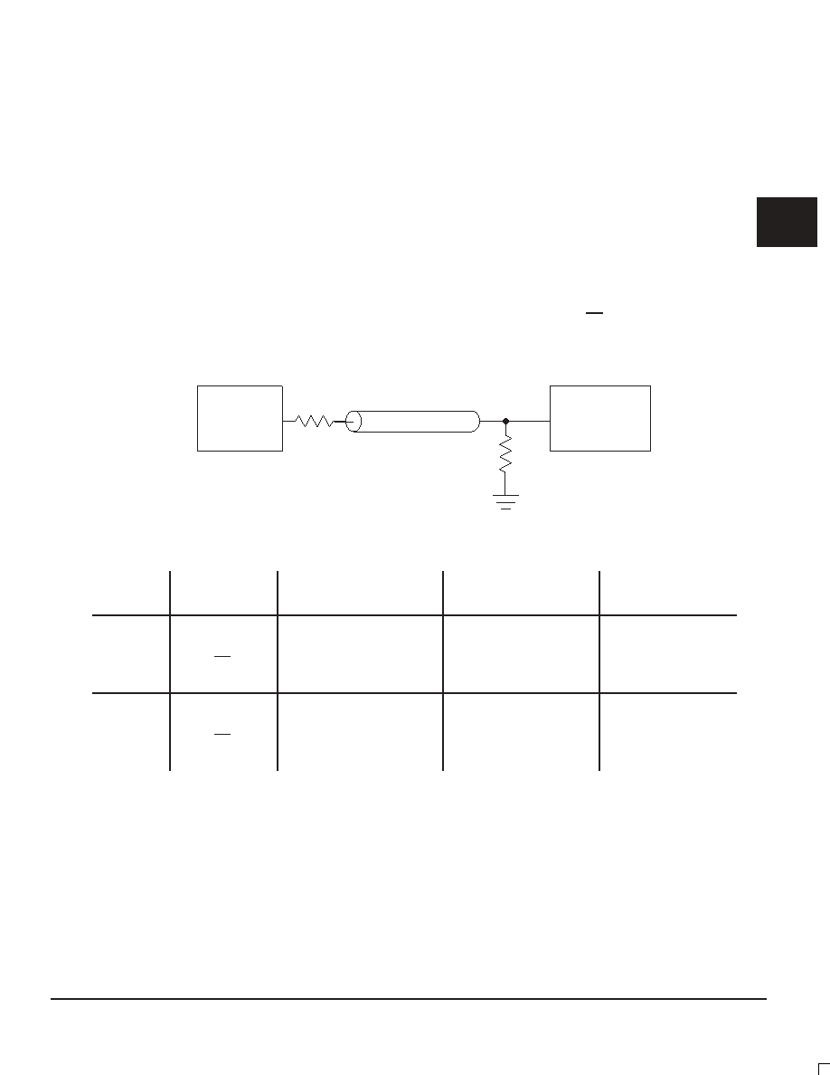
2. These two specs (tRlSE/FALL and tPULSE Width 2X_Q output)
guarantee that the MC88915T meets the 40MHz and
33MHz MC68040 P–Clock input specification (at 80MHz
and 66MHz, respectively). For these two specs to be
guaranteed by Motorola, the termination scheme shown
below in Figure 1 must be used.
3. The wiring Diagrams and explanations in Figure 5
demonstrate the input and output frequency relationships
for three possible feedback configurations. The allowable
SYNC input range for each case is also indicated. There
are two allowable SYNC frequency ranges, depending
whether FREQ_SEL is high or low. Although not shown, it
is possible to feed back the Q5 output, thus creating a 180
°
phase shift between the SYNC input and the “Q” outputs.
Table 1 below summarizes the allowable SYNC frequency
range for each possible configuration.
88915
2X_Q
Output
Rs
ZO (CLOCK TRACE)
68040
P-Clock
Input
Rs = Zo - 7
Figure 1. MC68040 P–Clock Input Termination Scheme
Rp = 1.5 Zo
Rp
Table 1. Allowable SYNC Input Frequency Ranges for Different Feedback Configurations.
FREQ_SEL
Level
Feedback
Output
Allowable SYNC Input
Frequency Range (MHZ)
Corresponding VCO
Frequency Range
Phase Relationships
of the “Q” Outputs
to Rising SYNC Edge
HIGH
Q/2
5 to (2X_Q FMAX Spec)/4
20 to (2X_Q FMAX Spec)
0
°
HIGH
Any “Q” (Q0–Q4)
10 to (2X_Q FMAX Spec)/2
20 to (2X_Q FMAX Spec)
0
°
HIGH
Q5
10 to (2X_Q FMAX Spec)/2
20 to (2X_Q FMAX Spec)
180
°
HIGH
2X_Q
20 to (2X_Q FMAX Spec)
0
°
LOW
Q/2
2.5 to (2X_Q FMAX Spec)/8
20 to (2X_Q FMAX Spec)
0
°
LOW
Any “Q” (Q0–Q4)
5 to (2X_Q FMAX Spec)/4
20 to (2X_Q FMAX Spec)
0
°
LOW
Q5
5 to (2X_Q FMAX Spec)/4
20 to (2X_Q FMAXSpec)
180
°
LOW
2X_Q
10 to (2X_Q FMAX Spec)/2
20 to (2X_Q FMAXSpec)
0
°
4. A 1M
resistor tied to either Analog VCC or Analog GND as
shown in Figure 2 is required to ensure no jitter is present
on the MC88915T outputs. This technique causes a phase
offset between the SYNC input and the output connected
to the FEEDBACK input, measured at the input pins. The
tPD spec describes how this offset varies with process,
temperature, and voltage. The specs were arrived at by
measuring the phase relationship for the 14 lots described
in note 1 while the part was in phase–locked operation. The
actual measurements were made with a 10MHz SYNC
input (1.0ns edge rate from 0.8V – 2.0V) with the Q/2 output
fed back. The phase measurements were made at 1.5V.
The Q/2 output was terminated at the FEEDBACK input
with 100
to VCC and 100 to ground.
2
相关PDF资料 |
PDF描述 |
|---|---|
| MC88915TFN55 | 88915 SERIES, PLL BASED CLOCK DRIVER, 7 TRUE OUTPUT(S), 1 INVERTED OUTPUT(S), PQCC28 |
| MC88915TFN70 | 88915 SERIES, PLL BASED CLOCK DRIVER, 7 TRUE OUTPUT(S), 1 INVERTED OUTPUT(S), PQCC28 |
| MC88916DW70 | 88916 SERIES, PLL BASED CLOCK DRIVER, 5 TRUE OUTPUT(S), 1 INVERTED OUTPUT(S), PDSO20 |
| MC88921DW | 88921 SERIES, PLL BASED CLOCK DRIVER, 5 TRUE OUTPUT(S), 0 INVERTED OUTPUT(S), PDSO20 |
| MC88LV915TFN | 88LV SERIES, PLL BASED CLOCK DRIVER, 7 TRUE OUTPUT(S), 1 INVERTED OUTPUT(S), PQCC28 |
相关代理商/技术参数 |
参数描述 |
|---|---|
| MC88915TFN55 | 功能描述:IC DRIVER CLK PLL 55MHZ 28-PLCC RoHS:否 类别:集成电路 (IC) >> 时钟/计时 - 时钟发生器,PLL,频率合成器 系列:- 标准包装:39 系列:- 类型:* PLL:带旁路 输入:时钟 输出:时钟 电路数:1 比率 - 输入:输出:1:10 差分 - 输入:输出:是/是 频率 - 最大:170MHz 除法器/乘法器:无/无 电源电压:2.375 V ~ 3.465 V 工作温度:0°C ~ 70°C 安装类型:* 封装/外壳:* 供应商设备封装:* 包装:* |
| MC88915TFN70 | 功能描述:IC DRIVER CLK PLL 70MHZ 28-PLCC RoHS:否 类别:集成电路 (IC) >> 时钟/计时 - 时钟发生器,PLL,频率合成器 系列:- 标准包装:39 系列:- 类型:* PLL:带旁路 输入:时钟 输出:时钟 电路数:1 比率 - 输入:输出:1:10 差分 - 输入:输出:是/是 频率 - 最大:170MHz 除法器/乘法器:无/无 电源电压:2.375 V ~ 3.465 V 工作温度:0°C ~ 70°C 安装类型:* 封装/外壳:* 供应商设备封装:* 包装:* |
| MC88915TFN70R2 | 功能描述:IC DRIVER CLK PLL 70MHZ 28-PLCC RoHS:否 类别:集成电路 (IC) >> 时钟/计时 - 时钟发生器,PLL,频率合成器 系列:- 标准包装:39 系列:- 类型:* PLL:带旁路 输入:时钟 输出:时钟 电路数:1 比率 - 输入:输出:1:10 差分 - 输入:输出:是/是 频率 - 最大:170MHz 除法器/乘法器:无/无 电源电压:2.375 V ~ 3.465 V 工作温度:0°C ~ 70°C 安装类型:* 封装/外壳:* 供应商设备封装:* 包装:* |
| MC88916 | 制造商:MOTOROLA 制造商全称:Motorola, Inc 功能描述:LOW SKEW CMOS PLL CLOCK DRIVER WITH PROCESSOR RESET |
| MC88916DW | 制造商:MOTOROLA 制造商全称:Motorola, Inc 功能描述:LOW SKEW CMOS PLL CLOCK DRIVER WITH PROCESSOR RESET |
发布紧急采购,3分钟左右您将得到回复。