- 您现在的位置:买卖IC网 > PDF目录11713 > MCZ33905S5EK (Freescale Semiconductor)IC SYSTEM BASIS CHIP GEN2 32SOIC PDF资料下载
参数资料
| 型号: | MCZ33905S5EK |
| 厂商: | Freescale Semiconductor |
| 文件页数: | 76/106页 |
| 文件大小: | 0K |
| 描述: | IC SYSTEM BASIS CHIP GEN2 32SOIC |
| 标准包装: | 42 |
| 应用: | 系统基础芯片 |
| 接口: | CAN,LIN |
| 电源电压: | 5.5 V ~ 27 V |
| 封装/外壳: | 32-BSOP(0.295",7.50mm 宽)裸露焊盘 |
| 供应商设备封装: | 32-SOICW 裸露焊盘 |
| 包装: | 管件 |
| 安装类型: | 表面贴装 |
第1页第2页第3页第4页第5页第6页第7页第8页第9页第10页第11页第12页第13页第14页第15页第16页第17页第18页第19页第20页第21页第22页第23页第24页第25页第26页第27页第28页第29页第30页第31页第32页第33页第34页第35页第36页第37页第38页第39页第40页第41页第42页第43页第44页第45页第46页第47页第48页第49页第50页第51页第52页第53页第54页第55页第56页第57页第58页第59页第60页第61页第62页第63页第64页第65页第66页第67页第68页第69页第70页第71页第72页第73页第74页第75页当前第76页第77页第78页第79页第80页第81页第82页第83页第84页第85页第86页第87页第88页第89页第90页第91页第92页第93页第94页第95页第96页第97页第98页第99页第100页第101页第102页第103页第104页第105页第106页
Analog Integrated Circuit Device Data
Freescale Semiconductor
71
33903/4/5
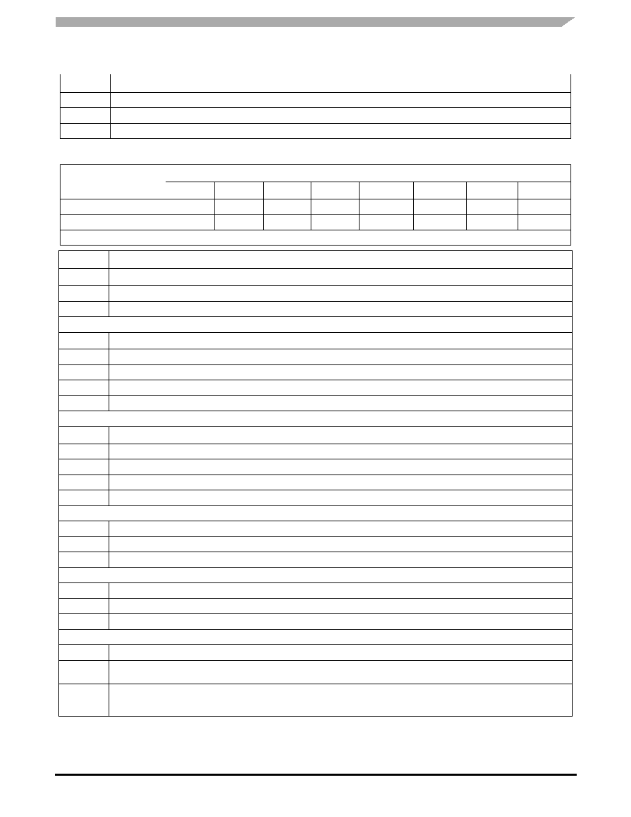
SERIAL PERIPHERAL INTERFACE
DETAIL OF CONTROL BITS AND REGISTER MAPPING
b0
Crank - Select the VSUP/1 threshold to disable VDD, while VSUP1 is falling toward GND
0
VDD disable when VSUP/1 is below typically 4.0 V (parameter VSUP-TH1), and device in Reset mode
1
VDD kept ON when VSUP/1 is below typically 4.0 V (parameter VSUP_TH1)
Table 19. Initialization LIN and I/O Registers, INIT LIN I/O (note: register can be written only in INIT mode)
MOSI First Byte [15-8]
[b_15 b_14] 0_0111 [P/N]
MOSI Second Byte, bits 7-0
bit 7
bit 6
bit 5
bit 4
bit 3
bit 2
bit 1
bit 0
01 00 _ 111 P
I/O-1 ovoff
LIN_T2[1]
LIN_T2[0]
LIN_T/1[1]
LIN_T/1[0]
I/O-1 out-en
I/O-0 out-en
Cyc_Inv
Default state
0
Condition for default
POR
Bit
Description
b7
I/O-1 ovoff - Select the deactivation of I/O-1 when VDD or VAUX overvoltage condition is detected
0
Disable I/O-1 turn off.
1
Enable I/O-1 turn off, when VDD or VAUX overvoltage condition is detected.
b6, b5
LIN_T2[1], LIN_T2[0] - Select pin operation as LIN Master pin switch or I/O
00
pin is OFF
01
pin operation as LIN Master pin switch
10
pin operation as I/O: HS switch and Wake-up input
11
N/A
b4, b3
LIN_T/1[1], LIN_T/1[0] - Select pin operation as LIN Master pin switch or I/O
00
pin is OFF
01
pin operation as LIN Master pin switch
10
pin operation as I/O: HS switch and Wake-up input
11
N/A
b2
I/O-1 out-en- Select the operation of the I/O-1 as output driver (HS, LS)
0
Disable HS and LS drivers of pin I/O-1. I/O-1 can only be used as input.
1
Enable HS and LS drivers of pin I/O-1. Pin can be used as input and output driver.
b1
I/O-0 out-en - Select the operation of the I/O-0 as output driver (HS, LS)
0
Disable HS and LS drivers of I/O-0 can only be used as input.
1
Enable HS and LS drivers of the I/O-0 pin. Pin can be used as input and output drivers.
b0
Cyc_Inv - Select I/O-0 operation in device LP mode, when cyclic sense is selected
0
During cyclic sense active time, I/O is set to the same state prior to entering in to LP mode. During cyclic sense off time, I/O-0 is disable (HS and
LS drivers OFF).
1
During cyclic sense active time, I/O is set to the same state prior to entering in to LP mode. During cyclic sense off time, the opposite driver of I/
O_0 is actively set. Example: If I/0_0 HS is ON during active time, then I/O_O LS is turned ON at expiration of the active time, for the duration of
the cyclic sense period.
Bit
Description
相关PDF资料 |
PDF描述 |
|---|---|
| V150C36H150BL2 | CONVERTER MOD DC/DC 36V 150W |
| C8051F985-GM | IC MCU 8BIT 2KB FLASH 20QFN |
| 901-9610-3SF | CONN SMA BULKHEAD JACK CRIMP |
| V150C36H150BF3 | CONVERTER MOD DC/DC 36V 150W |
| V24A28E500BF3 | CONVERTER MOD DC/DC 28V 500W |
相关代理商/技术参数 |
参数描述 |
|---|---|
| MCZ33905S5EK/R2 | 制造商:Freescale Semiconductor 功能描述:IC SBC GEN2 CAN LIN X1 32SOIC 制造商:Freescale Semiconductor 功能描述:IC, SBC, GEN2, CAN, LIN X1, 32SOIC |
| MCZ33905S5EKR2 | 功能描述:CAN 接口集成电路 5V SBC HSCAN SNGL LIN RoHS:否 制造商:Texas Instruments 类型:Transceivers 工作电源电压:5 V 电源电流: 工作温度范围:- 40 C to + 85 C 封装 / 箱体:SOIC-8 封装:Tube |
| MCZ33905S5R2 | 制造商:FREESCALE 制造商全称:Freescale Semiconductor, Inc 功能描述:SBC Gen2 with CAN High Speed and LIN Interface |
| MCZ33927EK | 功能描述:功率驱动器IC THREE PHASE PRE- DRIVER RoHS:否 制造商:Micrel 产品:MOSFET Gate Drivers 类型:Low Cost High or Low Side MOSFET Driver 上升时间: 下降时间: 电源电压-最大:30 V 电源电压-最小:2.75 V 电源电流: 最大功率耗散: 最大工作温度:+ 85 C 安装风格:SMD/SMT 封装 / 箱体:SOIC-8 封装:Tube |
| MCZ33927EK/R2 | 制造商:FREESCALE 制造商全称:Freescale Semiconductor, Inc 功能描述:Three-Phase Field Effect Transistor Pre-Driver |
发布紧急采购,3分钟左右您将得到回复。