- 您现在的位置:买卖IC网 > PDF目录17039 > MPC8313E-RDBB (Freescale Semiconductor)BOARD CPU 8313E VER 2.1 PDF资料下载
参数资料
| 型号: | MPC8313E-RDBB |
| 厂商: | Freescale Semiconductor |
| 文件页数: | 32/99页 |
| 文件大小: | 0K |
| 描述: | BOARD CPU 8313E VER 2.1 |
| 标准包装: | 1 |
| 系列: | PowerQUICC II™ PRO |
| 类型: | MPU |
| 适用于相关产品: | MPC8313E |
| 所含物品: | 板 |
第1页第2页第3页第4页第5页第6页第7页第8页第9页第10页第11页第12页第13页第14页第15页第16页第17页第18页第19页第20页第21页第22页第23页第24页第25页第26页第27页第28页第29页第30页第31页当前第32页第33页第34页第35页第36页第37页第38页第39页第40页第41页第42页第43页第44页第45页第46页第47页第48页第49页第50页第51页第52页第53页第54页第55页第56页第57页第58页第59页第60页第61页第62页第63页第64页第65页第66页第67页第68页第69页第70页第71页第72页第73页第74页第75页第76页第77页第78页第79页第80页第81页第82页第83页第84页第85页第86页第87页第88页第89页第90页第91页第92页第93页第94页第95页第96页第97页第98页第99页
MPC8313E PowerQUICC II Pro Processor Hardware Specifications, Rev. 4
38
Freescale Semiconductor
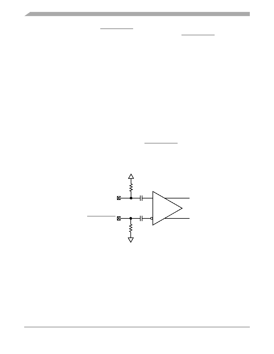
— The SD_REF_CLK and SD_REF_CLK are internally AC-coupled differential inputs as shown
in Figure 23. Each differential clock input (SD_REF_CLK or SD_REF_CLK) has a 50-
termination to XCOREVSS followed by on-chip AC coupling.
— The external reference clock driver must be able to drive this termination.
— The SerDes reference clock input can be either differential or single-ended. Refer to the
differential mode and single-ended mode description below for further detailed requirements.
The maximum average current requirement that also determines the common mode voltage range:
— When the SerDes reference clock differential inputs are DC coupled externally with the clock
driver chip, the maximum average current allowed for each input pin is 8 mA. In this case, the
exact common mode input voltage is not critical as long as it is within the range allowed by the
maximum average current of 8 mA (refer to the following bullet for more detail), since the
input is AC-coupled on-chip.
— This current limitation sets the maximum common mode input voltage to be less than 0.4 V
(0.4 V/50 = 8 mA) while the minimum common mode input level is 0.1 V above XCOREVSS.
For example, a clock with a 50/50 duty cycle can be produced by a clock driver with output
driven by its current source from 0 to 16 mA (0–0.8 V), such that each phase of the differential
input has a single-ended swing from 0 V to 800 mV with the common mode voltage at 400 mV.
— If the device driving the SD_REF_CLK and SD_REF_CLK inputs cannot drive 50
to
XCOREVSS DC, or it exceeds the maximum input current limitations, then it must be
AC-coupled off-chip.
The input amplitude requirement. This requirement is described in detail in the following sections.
Figure 23. Receiver of SerDes Reference Clocks
9.2.2
DC Level Requirement for SerDes Reference Clocks
The DC level requirement for the MPC8313E SerDes reference clock inputs is different depending on the
signaling mode used to connect the clock driver chip and SerDes reference clock inputs as described
below.
Differential mode
— The input amplitude of the differential clock must be between 400 and 1600 mV differential
peak-to-peak (or between 200 and 800 mV differential peak). In other words, each signal wire
Input
Amp
50
50
SDn_REF_CLK
相关PDF资料 |
PDF描述 |
|---|---|
| STD12W-T | WIRE & CABLE MARKERS |
| STD12W-X | WIRE & CABLE MARKERS |
| STD12W-F | WIRE & CABLE MARKERS |
| STD12W-G | WIRE & CABLE MARKERS |
| 0210490261 | CABLE JUMPER 1.25MM .102M 20POS |
相关代理商/技术参数 |
参数描述 |
|---|---|
| MPC8313E-RDBB | 制造商:Freescale Semiconductor 功能描述:; LEADED PROCESS COMPATIBLE:YES; PEAK RE |
| MPC8313E-RDBC | 功能描述:开发板和工具包 - 其他处理器 8313E CPU board Ver 2.2 RoHS:否 制造商:Freescale Semiconductor 产品:Development Systems 工具用于评估:P3041 核心:e500mc 接口类型:I2C, SPI, USB 工作电源电压: |
| MPC8313EVRADD | 制造商:Freescale Semiconductor 功能描述:MPC83XX RISC 32-BIT 90NM 333MHZ 1V/1.8V/2.5V/3.3V 516-PIN TE - Trays |
| MPC8313EVRADDB | 功能描述:微处理器 - MPU PBGA W/ ENCR RoHS:否 制造商:Atmel 处理器系列:SAMA5D31 核心:ARM Cortex A5 数据总线宽度:32 bit 最大时钟频率:536 MHz 程序存储器大小:32 KB 数据 RAM 大小:128 KB 接口类型:CAN, Ethernet, LIN, SPI,TWI, UART, USB 工作电源电压:1.8 V to 3.3 V 最大工作温度:+ 85 C 安装风格:SMD/SMT 封装 / 箱体:FBGA-324 |
| MPC8313EVRADDC | 功能描述:微处理器 - MPU 8313 REV2.2 W/ENC RoHS:否 制造商:Atmel 处理器系列:SAMA5D31 核心:ARM Cortex A5 数据总线宽度:32 bit 最大时钟频率:536 MHz 程序存储器大小:32 KB 数据 RAM 大小:128 KB 接口类型:CAN, Ethernet, LIN, SPI,TWI, UART, USB 工作电源电压:1.8 V to 3.3 V 最大工作温度:+ 85 C 安装风格:SMD/SMT 封装 / 箱体:FBGA-324 |
发布紧急采购,3分钟左右您将得到回复。